0
\$\begingroup\$

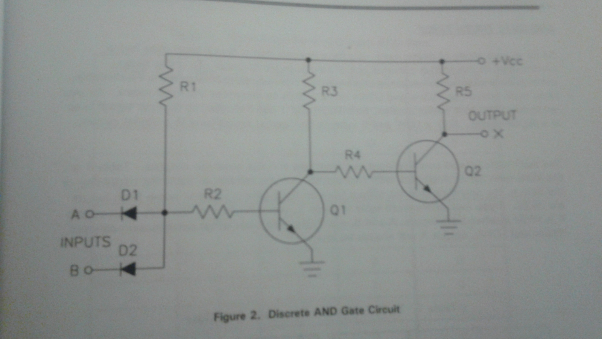
I am learning about the "AND" gate function in Navy school. What I know is that when a low voltage is at the base of Q1, the transistor is in cutoff mode since the collector is reading high (> 2 volts). This drives Q2 into saturation mode, meaning that its collector is reading a low close to 0 volts.

This is the accompanying image that I'm talking about: enter image description here

I was wondering if someone could show me the math involved in all this. For example, if I applied 2.8 volts on test point A and 0.7 volts on test point B, then what is the predicted output voltage at test point X (reading off from Q2)? What diodes' resistance and resistors' resistance are needed for the "and" function? I should get a low, but I need to see the math.

In my textbook, it says that when the diodes are reversed we get the "OR" function so I know that the diodes play a role in the calculations.

\$\endgroup\$

3 Answers 3

2
\$\begingroup\$

This is an example of DTL (diode-transistor logic). The Minuteman II missile, designed in the early 1960's, used 2000 DTL and DL IC's in its guidance computer. Diode logic (DL) performed its functions with just diodes and resistors, but since it lacked transistors for signal restoration you couldn't cascade many circuits together (or invert a signal).

Here is the truth table for an AND gate:

A  B  out

0  0   0
0  1   0
1  0   0
1  1   1

Now lets look at that in terms of voltages:

A  B      junction of R1 and R2

gnd  gnd  0.7     Q1 off, Q2 on (x = 0.7v)

gnd  Vcc  0.7     Q1 off, Q2 on (x = 0.7v)

Vcc  gnd  0.7     Q1 off, Q2 on (x = 0.7v)

Vcc  Vcc  ~Vcc    Q1 on, Q2 off (x = ~Vcc)

If either or both inputs A or B are ground (or close to it), the diode(s) associated with the grounded inputs will conduct, causing the voltage of the junction between R1 and R2 to be at around 0.7v, the forward voltage drop of the diodes.

Therefore the base voltage will be too low to turn Q1 on. The base of Q2 will be near Vcc, so it will turn on and the output X will be low, near the Vbe of Q1.

If both inputs A and B are near Vcc, both diodes will be reversed biased. The junction of R1 and R2 will then be near Vcc, and Q1 will turn on. This will put a near ground (Vbe of Q1) on the base of Q2, turning it off. So the output will then be high, near Vcc.

An OR gate is very similar. The diodes just face the other way, and R1 is connected to ground instead of Vcc.

Here is the truth table for an OR gate:

A  B  out

0  0   0
0  1   1
1  0   1
1  1   1

Now lets look at that in terms of voltages:

A  B      junction of R1 and R2

gnd  gnd  0.7        Q1 off, Q2 on (x = 0.7v)

gnd  Vcc  Vcc-0.7    Q1 on, Q2 off (x = ~Vcc)

Vcc  gnd  Vcc-0.7    Q1 on, Q2 off (x = ~Vcc)

Vcc  Vcc  Vcc-0.7    Q1 on, Q2 off (x = ~Vcc)

If either of the inputs are high, then the associated diode will be forward biased, and the voltage at the junction of R1 and R2 will be equal to the Vcc minus the diode drop.

The remaining analysis (what the output is depending on the voltage to the base of Q1) remains the same as for the AND gate.
\$\endgroup\$
2
  • \$\begingroup\$ I have a question, how could the junction between R1 and R2 be 0.7 but Q1 is off? \$\endgroup\$ Commented Nov 28, 2014 at 5:52
  • \$\begingroup\$ @newbie If the voltage at the base resistor R2 is only 0.7v, then the transistor is not going to turn on. There will essentially be no current through R2. You need to have enough current through R2 to saturate the transistor to turn it on. \$\endgroup\$
    – tcrosley
    Commented Nov 28, 2014 at 6:07
1
\$\begingroup\$

The AND function is performed by the diodes. Everything else is just amplification. Don't think about the "resistance" of the diodes. A diode is conducting or it's not. And when it is conducting there is a 0.7 volt drop across it.

If one of the inputs is low (say zero volts) then that diode will conduct, turning off Q1.

And, if the diodes are reversed the OR function is performed by the diodes. Everything else is just amplification.

\$\endgroup\$
0
\$\begingroup\$

It's math is nothing special but normal BJT amplifier's . If you put low voltage in any node (A or B) then that will on the diode and voltage at the node between \$R_1\$ and \$R_2\$ will be approximately 0.7 volt higher then the applied voltage which should results in turning off \$Q_1\$ . so current go through the \$R_4\$ higher which cause \$Q_2\$ run in saturation mood (so output voltage is approximately 0.2 volt).

If you apply higher voltage at inputs then max current goes through the \$R_1\$ (depending on your resistance value ) which should run \$Q_1\$ in saturation . so voltage at the node between \$R_3\$ and \$R_4\$ will be approximately 0.2 which will cut off \$Q_2\$ . So your output voltage will approximately \$V_{CC}\$

Hint's for your math :

to calculate accurate output you need to know \beta of the transistors and values of resistances.

let, \$V_(12) =\$ voltage at the node between \$R_1\$ and \$R_2\$

first consider voltage \$V_(12) =\$ if those diodes are not in circuit .

$$ V_(12) = \frac{(V_{cc} - 0.7)*R_2}{R_2+R_1}$$

if this voltage is higher then any of your input+ 0.7 volt then you can consider that diode on and take voltage at \$V_(12)\$ = input+0.7 and calculate the rest of amplifier circuit .

if the voltage is not higher then input + 0.7 volt then you can use calculated value to solve the amplifier circuit .

Hope you know how to solve BJT amplifier circuit . Best of luck .

\$\endgroup\$

Your Answer

By clicking “Post Your Answer”, you agree to our terms of service and acknowledge you have read our privacy policy.

Not the answer you're looking for? Browse other questions tagged or ask your own question.