2
\$\begingroup\$

I have a question regarding sending a short duration signal from a faster clock domain to a slower clock domain. I am trying to implement a dual frame buffer in a dual port (dual clock) RAM. Once an entire Frame has been stored, the write clock side asserts the FrameFull register. At the end of each current display frame, the display requests a new frame, which if available, sets the read pointer for the RAM accordingly and is also used to deassert the FrameFull Signal so that a new frame can be loaded while this most recent one is being displayed.

The read side is operating at 50 MHz.
The write side is operating at 27 MHz.

In order to synchronize the FrameFull Signal from the write domain, I have read that its best to use a couple of synchronizing flip flops and since the FrameFull remains asserted until the buffer is switched, I think this isn't very problematic (because the FrameFull signal can't be missed). The SwitchSuccesful signal is asserted in the read clock domain when a new Frame is requested and the FrameFull is 1, indicating buffer exchange. Now, this SwitchSuccesful needs to be sampled by the write domain so that FrameFull can be reset to 0 and can then start storing a new frame. I have thought about it and decided to use a 16-bit shift register, which, when buffers are switched, will reset to 16'hFF and then shift left with a zero being concatenated.I could then use a bitwise OR, and synchronize the result of the bitwise OR with Flip Flops in the write domain before sampling the signal. Will this be sufficient to prevent missing the SuccesfulSwitch and metastability?

CODE :

always @ (posedge read_clock)
begin
    if(SwitchRequest) begin
          case (Frame_FullSync1, Frame_Read) 
          2'b00 : begin rd_ptr <= /*Some Value*/ Frame_Read <= 0; end           //Restore to Previous 0.
          2'b01 : begin rd_ptr <= /*Some Value*/ Frame_Read <= 1; end           //Restore to Previous 1.
          2'b10 : begin rd_ptr <= /*Some Value*/ Frame_Read <= 1; LE <= 1; end  //Load new ----- 0 to 1.
          2'b11 : begin rd_ptr <= /*Some Value*/ Frame_Read <= 0; LE <= 1; end  //Load new ----- 1 to 0.
          endcase
    end
    if(LE) LE <= 0;
end

always @ (posedge read_clock)  begin 
    //Frame Full Synchronization from write domain to read domain
    Frame_FullSync1 <= Frame_FullSync0;
    Frame_FullSync0 <= FrameFull;
    //LE was asserted for 1 clock cycle when buffer switch was succesful
    if(LE) Sync <= 16'hFF;
    else   Sync <= Sync {Sync[15 : 1],1'b0};
end

assign SwitchSuccesful = |Sync;

always @ (posedge write_clock) begin
    //Synchronization of bitwise OR
    SwitchSuccesfulSync0 <= SwitchSuccesful;
    SwitchSuccesfulSync1 <= SwitchSuccesfulSync0; 
end
\$\endgroup\$
5
  • 2
    \$\begingroup\$ A 16 bit SR seems overkill. A two clock width pulse from the 27MHz domain will be read without no doubt by a two FF synchronyzer from the 50MHz domain. \$\endgroup\$ Commented Apr 12, 2017 at 16:58
  • \$\begingroup\$ Thank you for the prompt reply! The output frame rate is 72 Hz, So, it doesn't cost much if I load a new image one frame later.So, you suggest that I should reduce the SR length and keep the bitwise OR(To produce n 50MHz cycles long pulses, provided that shift register lenth = n )? \$\endgroup\$ Commented Apr 12, 2017 at 17:04
  • 1
    \$\begingroup\$ I see no real issues with a two or three FF SR. Bitwise OR... and then probably an edge detector to get a neat one pulse width signal in the fast domain. \$\endgroup\$ Commented Apr 12, 2017 at 17:09
  • 2
    \$\begingroup\$ I suggest reading this paper on clock domain crossing (CDC): sunburst-design.com/papers/CummingsSNUG2008Boston_CDC.pdf \$\endgroup\$
    – Greg
    Commented Apr 12, 2017 at 17:16
  • \$\begingroup\$ "One potential solution to this problem is to assert CDC signals for a period of time that exceeds the cycle time of the sampling clock as shown in Figure 10. As discussed in section 4.1.1, the minimum pulse width is 1.5X the period of the receiving clock frequency. The assumption is that the CDC signal will be sampled at least once and possibly twice by the receiver clock. Open-loop sampling can be used when relative clock frequencies are fixed and properly analyzed." Excellent Paper.I have gone through bits of it, but the part quoted above seems to reinforce Mr.Claudio's point. \$\endgroup\$ Commented Apr 12, 2017 at 17:31

3 Answers 3

5
\$\begingroup\$

Assuming the data of interest changes on the falling edge of the 27Mhz clock and is sampled on the rising edge, the approach with minimal delay would be to have a divide-by-two clocked by the 27MHz clock whose output flips on the rising edge, feed the output of that into a double synchronizer which samples on the falling edge of the 50MHz clock, and capture everything else on the rising edge of the 50MHz clock.

If two consecutive falling edges of the 50Mhz clock report opposite states for the divide-by-two output, that implies that the real edge must have happened somewhere within that interval. The data will have been sampled at a time halfway between those 50MHz clock events, within about 10ns of when the 27MHz clock occurred.

Sampling everything on the same edge of the 50MHz clock may not be sufficient to allow reliable decoding of events. Consider the following two scenarios, with the first line representing 50MHz clock events and the latter representing 30MHz clock events (the same principles would apply at 27); both lines have a scale of 3.3ns per character

|-----|-----|-----|-----|-----|--  -- 50Mhz clock rising edges
-|---------|---------|---------|-  -- 30Mhz clock rising edges
_x---------x_________x---------x_  -- 30MHz/2, changing on rising edges
______x---------x_________x------  -- 30MHz/2, changing on falling edges
000000x111111111x222222222x333333  -- Data words, changing on 30Mhz fall

Consecutive samples of the divided 30Mhz clocks and data words would yield:

_-__--_--_  30MHz/2, changing on rising edges, then sampled @50Mhz rising
_x-__-x_--  30MHz/2, changing on falling edges, then sampled @50Mhz rising
0x1223x455  Data, sampled @50Mhz rising

There is no spot relative to observed edges on either form of the 30MHz clock where the output would be guaranteed to be clean. On the other hand, if the "30Mhz/2 rising" signal were sampled on falling edges of the 50Mhz clock, that would yield, relative to the data:

--_x-__-x_  30Mhz/2, changing on rising edges, sampled @50Mhz falling
0x1223x455  Data, sampled @50Mhz rising

If a 30Mhz clock coincided with a falling edge of the 50Mhz clock, there may be 20ns worth of uncertainty as to when the edge occurred, but the same data would be present on the cycles before and after, so such uncertainty wouldn't matter.

\$\endgroup\$
11
  • \$\begingroup\$ I might need some time to catch up with what's being said here, but in a nutshell, the signal is asserted on the positive edge of the 50Mhz clock domain and all of the sampling in the 27Mhz too takes place on the positive edge of the clock. \$\endgroup\$ Commented Apr 12, 2017 at 17:41
  • \$\begingroup\$ @AhmedAliAbbasi: If you can operate some clocks on the opposite edge of the 50MHz clock that will make it easier to get reliable operation. If 50MHz clock cycle T shows that a 27MHz edge has occurred, it's possible that the edge had actually occurred almost 20ns earlier or 20ns later, so unless the 27MHz signal would satisfy 20ns sample and hold times (which it couldn't if each clock represented another word, since sample and hold combined can't exceed the 37ns word time). \$\endgroup\$
    – supercat
    Commented Apr 12, 2017 at 18:41
  • \$\begingroup\$ @AhmedAliAbbasi: I added more explanation and some timing diagrams to show why it could likely be necessary to have some latches clocked on the opposite edge of the 50MHz clock. \$\endgroup\$
    – supercat
    Commented Apr 12, 2017 at 19:15
  • \$\begingroup\$ Perhaps the fact that the signal that crosses from the 27 Mhz domain to the 50 Mhz domain REMAINS asserted until it is acknowledged in the 50Mhz domain eases things a little.Because even if I do not sample the 27Mhz signal as soon as possible in the 50Mhz domain, the design shouldn't run into much trouble. \$\endgroup\$ Commented Apr 12, 2017 at 19:16
  • \$\begingroup\$ I see, Thank you for taking out the time! I am sure they'll go a long way in helping me understand all this. Regards, \$\endgroup\$ Commented Apr 12, 2017 at 19:19
1
\$\begingroup\$

I couldn't exactly follow the entire scenario you described, but if the question just boils down to "what's a good way to pass a single clock cycle pulse into a different clock domain", considered this: Instead of generating a pulse, simply toggle the signal. Pass this toggled signal into the other clock domain using meta-stability registers. In the other clock domain, implement an edge detection circuit that will generate a single clock cycle pulse on level changes. That's it, pulse passed. This will only work reliably if the signal changes relatively infrequently (I'd say a maximum frequency of once every 4 of the slower clock cycles) in order to let the meta-stability registers settle out.

\$\endgroup\$
2
  • \$\begingroup\$ You have understood the question ; that is exactly what I wanted to ask.(I think I need to be more concise and accurate in my descriptions). However, If I a generate an edge/toggle (1 clock cycle in the faster domain), isn't there the chance that either a) the signal toggles and settles back to the original value before the sampling edge of the slower clock domain? b) the metastable signal settles to a false value (that is 0 when actual sample was 1, 1 when actual sample was 0)? Thank you! \$\endgroup\$ Commented Apr 13, 2017 at 19:12
  • \$\begingroup\$ That is why I made the statement about the input/fast signal must can only toggle once every few slower clock cycles. The input must toggle, and then maintain that state for several slow clock cycles. This will guarantee that the meta-stability registers have a constant level input, to avoid the scenario of "missing" the edge. \$\endgroup\$ Commented Apr 16, 2017 at 18:05
1
\$\begingroup\$

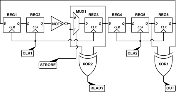
Since the person asking the original question has clarified that the RAM can use independent clocks for writing and reading, I would like to suggest a nice approach for passing events between clock domains: construct a ring of flip flops, with two or three in each domain, one inversion going around the ring, and a latch-enable on one of the flops in the sending domain. Something like:

schematic

simulate this circuit – Schematic created using CircuitLab

(I used a D flop and a mux to simulate a D flop with latch-enable control).

READY will be high when the device is ready for an event in the source domain. After a source-domain clock cycle where STROBE and READY are both high, READY will go low and remain low until the event has been processed and acknowledged. The OUT signal in the destination clock domain will be high for exactly one clock cycle in that domain after an event is triggered. Note that even if the source clock were to stop on the cycle after STROBE and READY were high, the event would still propagate to the destination domain. The circuit could be made to allow faster turnaround time on events, by feeding REG1 off REG5 rather than REG6, and moving REG2 to the output of XOR2 (to avoid metastability, there should be two CLK1-based flops between the REG6 signal and the READY output, but one of them could be after the XOR). I think the behavior of the circuit as drawn is probably less confusing. The left domain will show "ready" if a strobe would be effective on the next cycle, and will not become ready again until the right-hand domain has actually had a clock cycle where OUT was high.

\$\endgroup\$
4
  • \$\begingroup\$ Does this pass timing analysis? \$\endgroup\$
    – user39382
    Commented Apr 14, 2017 at 5:33
  • \$\begingroup\$ @duskwuff: Each signal that passes between clock domains passes through two registers in the new domain before going anywhere else. The reason for using a double-synchronizer is that if an input violates setup/hold constraints of the first register, its output might do anything but would be unlikely to do so in a fashion that would cause the second to do anything other than latch a clean high or a clean low. Timing analysis tools mwy need to be told to presume that the output from the first register in each pair would satisfy the constraints of the second. \$\endgroup\$
    – supercat
    Commented Apr 14, 2017 at 16:58
  • \$\begingroup\$ @duskwuff: Such presumptions are in a sense "cheating", since any circuit could be made to pass timing analysis if the timing analyzer is told to assume that critical parts will magically work. On the other hand, it would be impossible to make any designs with independent dual clocks pass timing analysis if the analyzer isn't willing to "trust" some kind of synchronizer. For some purposes it might not be a bad idea to add another layer of synchronization on each side to reduce the probability of errant behavior (cheap insurance, if propagation delay isn't a concern), but... \$\endgroup\$
    – supercat
    Commented Apr 14, 2017 at 17:01
  • \$\begingroup\$ ...that would depend upon what was being controlled and the consequences of any possible errant behaviors. \$\endgroup\$
    – supercat
    Commented Apr 14, 2017 at 17:02

Your Answer

By clicking “Post Your Answer”, you agree to our terms of service and acknowledge you have read our privacy policy.

Not the answer you're looking for? Browse other questions tagged or ask your own question.