1
\$\begingroup\$

I'm going to print my first PCB wich is a small controller, nothing complicated. I know that I need to output GERBER or GERBER-X2 files. I prefer GERBERX2 because it comes with the board outline for the manufacturer.

My problem is the following:

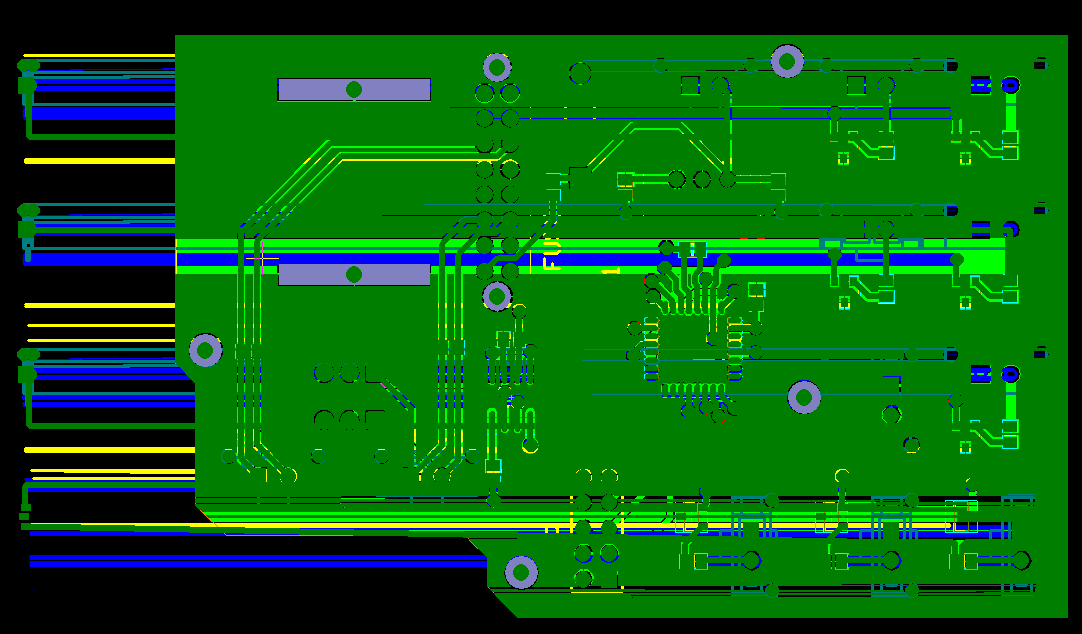
Here is the CAMtastic file altium produces: enter image description here
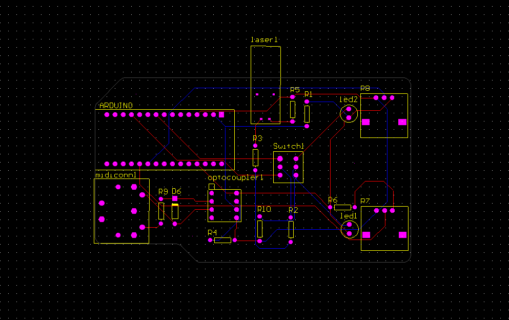
But when I export that file to a Gerber file and I open it in Altium, it produces that:enter image description here
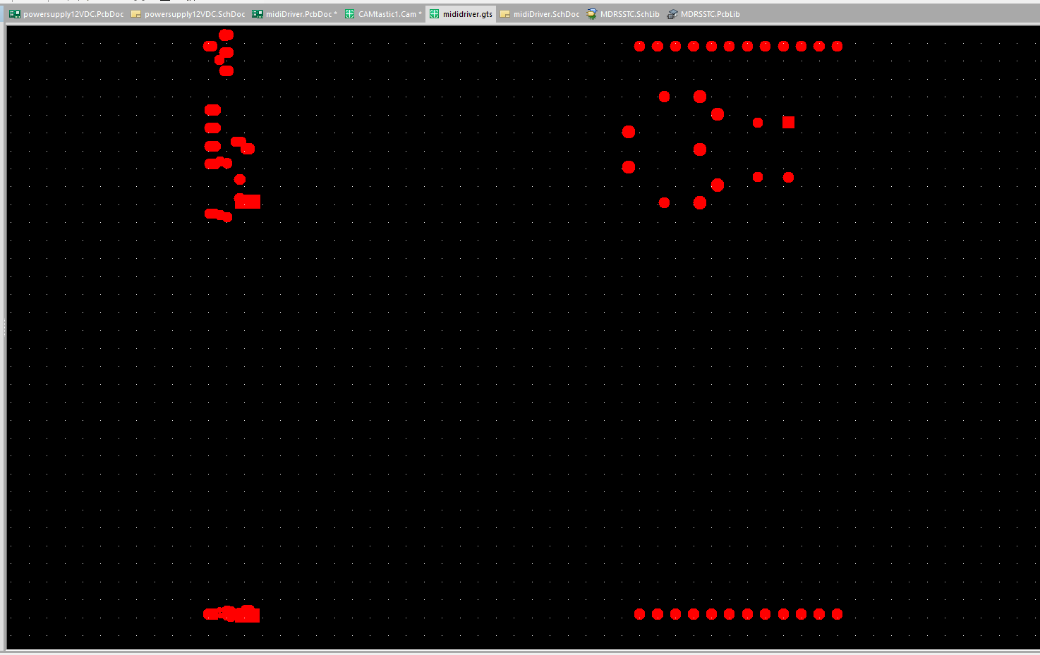
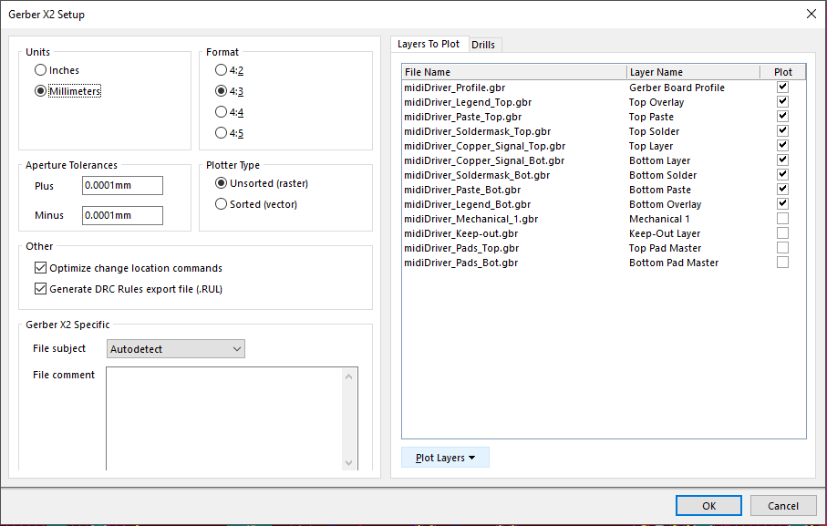
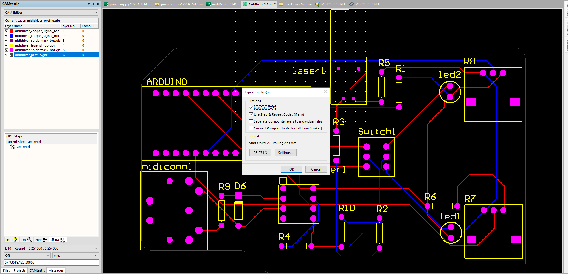
I followed instruction on youtube videos for the settings. Here they are: enter image description here
Then I export the CAMtastic file as gerber with those settings: enter image description here Every layer is wrong! I don't understand. Is altium corrupted?
\$\endgroup\$
3
  • \$\begingroup\$ Can you please show us the settings? \$\endgroup\$
    – DerStrom8
    Commented Sep 11, 2017 at 11:58
  • \$\begingroup\$ i'll add them in my Question \$\endgroup\$
    – PyThagoras
    Commented Sep 11, 2017 at 19:49
  • \$\begingroup\$ I generally use an OutJob. It's much more user-friendly than CAMTastic. \$\endgroup\$
    – DerStrom8
    Commented Sep 11, 2017 at 20:29

2 Answers 2

4
\$\begingroup\$

When you view the files in Camtastic, you are already viewing the Gerber files. Camtastic is a "Gerber File Viewer and Editor".

You do not need to export anything from Camtastic.

After you generate the Gerber files (typically done using an 'OutJob' file), simply open the output folder in your project files (using windows explorer), and zip up the output files you need to send to your pcb manufacturer.

You can use Camtastic to view the generated Gerber files, and pseudo-independently confirm that they are ok and conform to some rules (see the Camtastic analysis menu).

Sometimes, in rare and advanced circumstances, one would want to edit Gerber data using Camtastic, and re-export using the tools in Camtastic program. However, this is really unusual now-a-days, and I have not had the need in a decade.

Camtastic can be used as part of the process to reverse engineer Gerber data back to a pcb file. But this also is an advanced and unusual requirement.

'OutJobs' are your friends. You'll be happier if you use them.

\$\endgroup\$
0
\$\begingroup\$

In my case, which was almost the same as yours, including polygon pours, I solved it by changing the PCB editor coordinates origin:

Edit >> Origin >> Set

That lead me to think it was caused by a non-rectangular/strange board cutout or shape

BEFORE: enter image description here

AFTER: enter image description here

\$\endgroup\$

Your Answer

By clicking “Post Your Answer”, you agree to our terms of service and acknowledge you have read our privacy policy.

Not the answer you're looking for? Browse other questions tagged or ask your own question.