9
\$\begingroup\$

I'm working on a board that has some LVDS 2.5 signals. All the guides I've read about board layout say not to put vias in between the differential traces, eg this guide

enter image description here

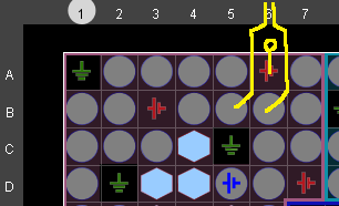
In a few cases it would be a lot easier to route the differential pairs out like this:

enter image description here

Looking at B5 and B6, they go around a power pad (with a via right next to it) and then continue together. I'd want to do that with a few ground pads also.

If I don't do that, I'll need either 3 mil trace and space instead of 5 mil, or a 6 layer board instead of 4 layer. Ouch.

So the question is, how bad is this really? Should I expect 10 mV coupled into the LVDS lines, or 100 mV?

The BGA is 1.0mm pitch, the traces are 7.7 mil spaced 5 mil apart for 100 ohm differential (but probably 5/5 while escaping the BGA). The top layer is signal, then ground 0.23 mm below that, then power. The BGA is an Artix-7 XC7A15T.

UPDATE The LVDS signals are clocked at 600MHz DDR.

UPDATE I'm more worried about current spikes on the power/ground coupling into the LVDS lines in different directions on each line, ie driving one line higher and the other lower, enough to cause the receiver to read the wrong (or indeterminate) value. Not so much about impedance discontinuity or reflections. But I really don't know... that's just intuition.

\$\endgroup\$
2
  • \$\begingroup\$ One of the golden rules of differential traces is both traces MUST have identical flight-times (length) and capacitive loading. If 500 MHZ to GHZ frequencies then this is mandatory. \$\endgroup\$
    – user105652
    Commented Mar 3, 2018 at 5:43
  • \$\begingroup\$ I would advise to take a look at application guides for the specific FPGA or IC, and examine their layout (frequently offered in development kits) for recommended break-out areas. \$\endgroup\$ Commented Mar 3, 2018 at 6:39

3 Answers 3

8
\$\begingroup\$

The short answer is that I'd argue that a spacing change near the start or end point of a differential signal is not that bad. I'd also argue that 6 layers is not that many. But at high speeds, definitely keep all noise sources away from the clock.

For the longer answer, let's look at the reasons given. The Toradex source you cite mentioned an impedance discontinuity, and EMC compliance.

The impedance discontinuity comes from the fact that, if there is a via between traces, the traces are at first have a capacitive coupling with each other, then that coupling is removed and replaced with the via, then they couple together again. Any impedance change will cause a reflection (see Impedance Mismatch). The ratio of reflection is: $$ \Gamma=\frac{Z_1-Z_2}{Z_1+Z_2} $$ Where Z is the impedance change. Note that the real impedance is different for different frequencies. So, we get signals reflecting back to the driver, potentially damaging the driver by forcing an over or under voltage condition (not very likely, particularly not with an FPGA's LVDS, which was relatively rugged when I used it, but reliability is important), and then it can reflect back again from the impedance change at the driver, and hit the receiver. Worst case, it destructively interferes with an edge and makes it non-monotonic.

What needs to happen for this worst case scenario? I believe the rule of thumb is that you are in trouble if the reflection distance is over 1/6 the fundamental wavelength. So, if your edge rate (not switching frequency, but the rise time of your edges) is 1 ns, we know electricity travels about 6 inches per ns in copper, so if the reflection distance is over 1 inch, you are on thin ice, and should look at how much the impedance is changing. Similarly, if the via is near the receiving side of the signal, I would argue that the impedance mismatch is going to get lost in the impedance mismatch inherent in reaching the receiver.

The second issue Toradex points to is EMC compliance, which is a bit of a fuzzy term. They could be worried about coupling or trace length mismatch. I don't think coupling is necessarily an issue; these are differential lines so the net coupling should cancel out, unless you are really pushing your voltage margins. Trace length mismatch could be more common if there is an obstruction in your traces, but it is not a necessary outcome.

To go a bit more into coupling, in the ideal case, if you couple the same signal into a differential pair, you would prefer to couple into both. Doing that would bump them both by a few mV, and the differential signal (Vp - Vn) would be unaffected. As long as the absolute voltages of each signal are within spec, you should be fine. At very high speeds you may run into an issue where the signal couples into one line slightly before it would couple into the other. This would be an issue, but I'd argue even here having the noise couple into both lines is better than having it couple into one, because either the noise is reduced by the differential nature, or you have two problems instead of one.

If you are dealing with something very high speed, with edge rates under 1 ns, then you should be explaining the answer to me, and you should probably use a board with more than 4 layers. If you're just trying to drive an 80 MSPS ADC, this advice should be solid. Keep in mind that edge sensitive lines, like clocks, are by far the most important signals to treat correctly.

One final tip: If the going gets tough, look into microvias which may be placed in the BGA pads.

\$\endgroup\$
4
  • 2
    \$\begingroup\$ +1, Excellent answer! One thing: SI symbol for seconds is "s," not "S," which is for Siemens. \$\endgroup\$
    – Shamtam
    Commented Mar 3, 2018 at 6:25
  • \$\begingroup\$ @pscheidler - Good answer. Yeah, the signals are fast, probably 0.2ns edges and 600MHz clock. But I have not much clue about LVDS :) I'm mostly worried about power/ground current spikes causing enough noise on LVDS to cause the wrong level to be received on the other side. \$\endgroup\$
    – Alex I
    Commented Mar 3, 2018 at 7:22
  • 1
    \$\begingroup\$ @AlexI I editted the answer to add a bit more on coupling. Be very careful with the clock and other edge sensitive lines. The good news about differential lines is that, if you match the lengths correctly, you should get no current spikes from driving the LVDS pair, because the net current should be consistent. You should also definitely use 6 layers, because you will want nice big ground planes to handle any current spikes your high speed IC do produce. Inter-plane capacitence is the only way to clean up very very high speed noise. But that's another issue and I've already rambled \$\endgroup\$
    – pscheidler
    Commented Mar 3, 2018 at 15:02
  • 1
    \$\begingroup\$ @Shamtam I have engineered for a long, long time, and I never new the SI unit for seconds, and I always called the inverse of Ohms Mhos! \$\endgroup\$
    – pscheidler
    Commented Mar 3, 2018 at 15:02
2
\$\begingroup\$

If you really need to know, you should look into simulation.

You should also edit your question to include the signaling speed or edge rate of the signals.

But I think there is a good chance you will get away with it. Diff pairs primarily couple to the adjacent plane. They don't couple edge-wise to each other very much. So the deviation in spacing will have minimal effect on the differential impedance. The critical thing for differential pairs is to match length.

A few times I have done boards where I violated spacing rules in one or two places to help escape from a BGA. This did not incur major cost increase for the board. This was in high volume production.

So you possibly can route most of the board using 5/5 rules, and use 3 mil spacing only in the area where you escape from the BGA. This may not be a problem for the board vendor. You could investigate that.

\$\endgroup\$
2
\$\begingroup\$

If that region of discontinuityis << wavelength, then you are OK.

If your edges are 1nanosecond Trise, Tfall, and that region of bad Z_diff is 50 picoseconds ( < 5% of the edge time) you will be OK.

And even the edge gets upset, the DATA EYE is what is important. 100pS upset in a 5nanosecond-long data-eye will be fine; the reflections will have long faded away before the receiver-clock strobes the receiver FlipFlop to make a decision.

=====================================

And if the reflections should occur in such a way as to increase the data-eye, like would be even better.

Beware of the signal energy stored in the ESD structures and the leadframe inductance of the package. Its is ISI -- inter Symbol Interference --- and may improve or may degrade the data-eye.

\$\endgroup\$

Your Answer

By clicking “Post Your Answer”, you agree to our terms of service and acknowledge you have read our privacy policy.

Not the answer you're looking for? Browse other questions tagged or ask your own question.