0
\$\begingroup\$

I have a big problem with Altium. To immune my board I want to place special VIA/Pads with hole on all the board (at the corner). I know this is possible with the tools "via stitching", but the tools doesn't work on my design (Altium PCB design: Vias stitching problem).

The idea is to place special EMC via on the board, but every time I update my PCB, all of my VIA are delete. Is there a possibility to tick an option for this component ? (I tried to change the type in "net tie " or "mechanical" but that doesn't work)

I don't want to place 50 specials via or emc schematic... enter image description here
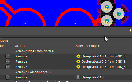
EDIT: A screen to show what I need to do: Three vias in triangle that will deacrese the impedance connection with the ground. On the screen I placed every signle VIA but it is very long and impossible to align with others..

enter image description here

Thanks for reading

\$\endgroup\$
5
  • \$\begingroup\$ Are you placing pads or vias? They are not the same thing. You should be using Place -> Via, not Place -> Pad \$\endgroup\$
    – DerStrom8
    Commented Apr 5, 2018 at 10:51
  • \$\begingroup\$ It is speical footprints that I created on my library. This footprint got an hole to link the bottom and the top ground (and also the ground plane inside my layers). I can't create a template because it is 3 pads to make a real good connection to the ground. \$\endgroup\$
    – JordanM67
    Commented Apr 5, 2018 at 12:23
  • \$\begingroup\$ Don't create a component just to place a pad/via. Just place the vias. \$\endgroup\$
    – DerStrom8
    Commented Apr 5, 2018 at 12:26
  • \$\begingroup\$ If I have to place each via with this solution, it will be long and not align. I need 3 via in triangle like on the picture, and then I have to align this triangle with others triangle. \$\endgroup\$
    – JordanM67
    Commented Apr 5, 2018 at 14:52
  • \$\begingroup\$ Haven't you heard of the "Align" feature and the copy/paste feature? Use the two together and you'll be all set. Create one cluster of three vias, highlight them, copy them, position/paste them, and repeat. \$\endgroup\$
    – DerStrom8
    Commented Apr 5, 2018 at 19:05

1 Answer 1

1
\$\begingroup\$

You could: Place the vias and lock the components (by checking the 'locked' box in the properties window with the PCB inspector) so the update won't change your vias.

Or you could change the DFM rules, (which I'm not too familiar with because I'm more of a schematics designer)

As far as alignment goes, use a grid or manually force one of the graphical locations (one row of vias has all the same X values, so you could align all of the X values by selecting a row and typing in and X value). I have used excel and copied in Y values with calculated offsets. With the PCB list its as simple as copying and pasting.

\$\endgroup\$

Your Answer

By clicking “Post Your Answer”, you agree to our terms of service and acknowledge you have read our privacy policy.

Not the answer you're looking for? Browse other questions tagged or ask your own question.