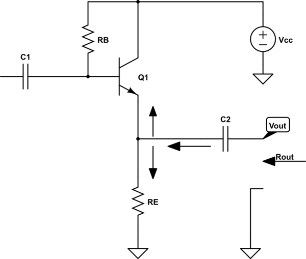
The simplest common collector amplifier looks like this:

simulate this circuit – Schematic created using CircuitLab
And now if we are looking form the load resistance perspective.
We see two paths for a current to flow.
One path is through the \$R_E\$ resistor into GND.
And the second path is into the transistor emitter terminal.
And this is why the load is seeing two "resistances" in parallel.
\$R_{OUT} = R_E||(r_e + \frac{R_B}{\beta+1})\$
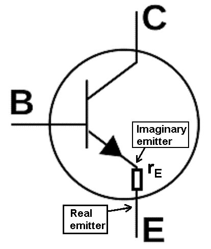
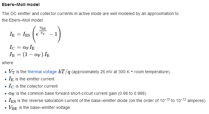
Where \$r_e = \frac{V_T}{I_E} \approx \frac{26mV}{I_E}\$
http://users.physics.harvard.edu/~horowitz/aoe/sm/smlitlre.htm
how to derive the ac emitter resistance of transistor amplifier biasing?
Or you can see it this way. The NPN transistor can only "source" the current into the load resistance. And \$R_E\$ resistor can "sink" the load current.
EDIT
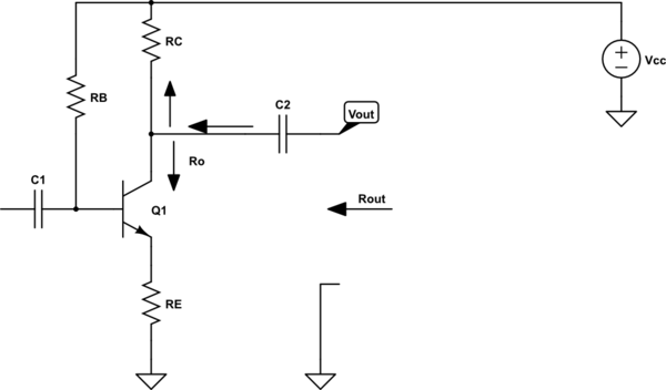
For the CE amplifier with emitter degeneration resistor (\$R_E\$), we have this situation:

simulate this circuit
And again we have two paths for a current.
But this time the resistance seen from the transistor collector into the transistor is very large and include the \$R_E\$ resistor.
\$\large R_O \approx r_o*(1+\frac{\beta*R_E}{(\beta+1)*r_e+R_B+R_E})\$
\$r_o\$ - https://en.wikipedia.org/wiki/Early_effect#Small-signal_model
So in practice, we write this like this:
\$R_{OUT} = R_C||R_O\$
And because \$R_C << R_O \$
\$ R_O = R_C||R_O \approx R_C\$

