The Miller plateau in a MOSFET circuit is flat and level when the drain current \$I_D\$ of the MOSFET is held constant (or nearly so) by the external circuit, and the MOSFET is operating in the saturated region.
Explanation and justification to come.
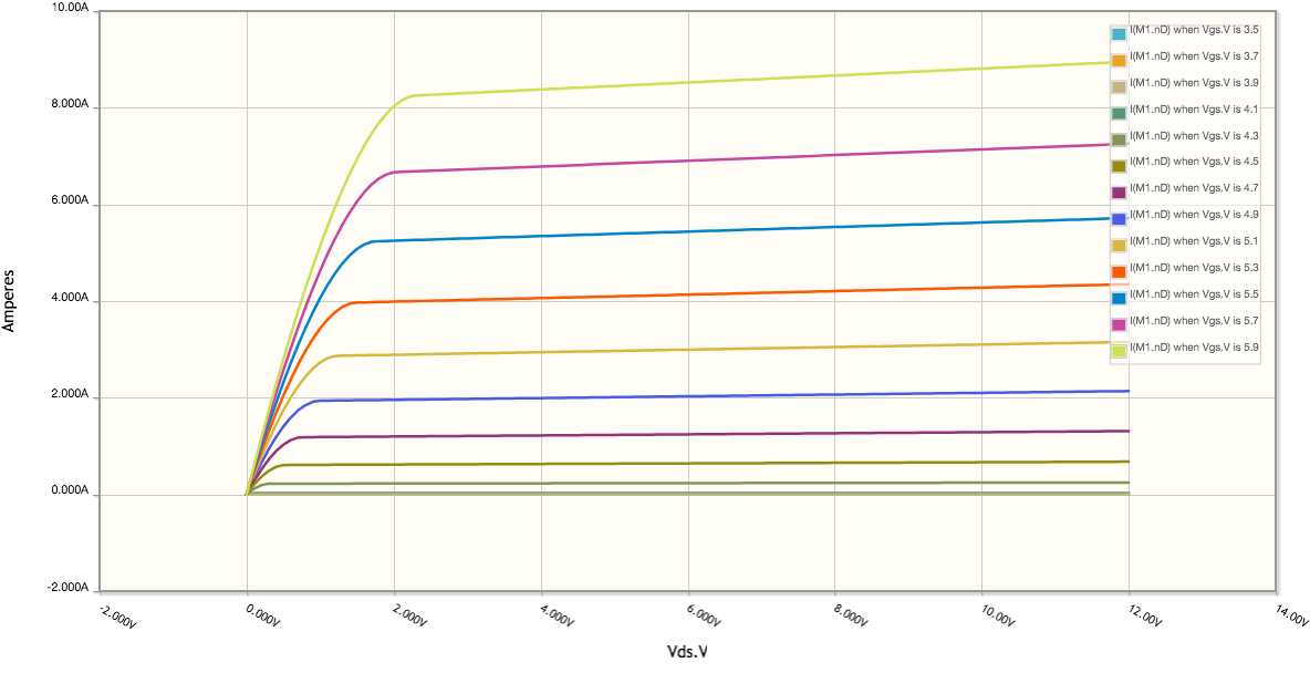
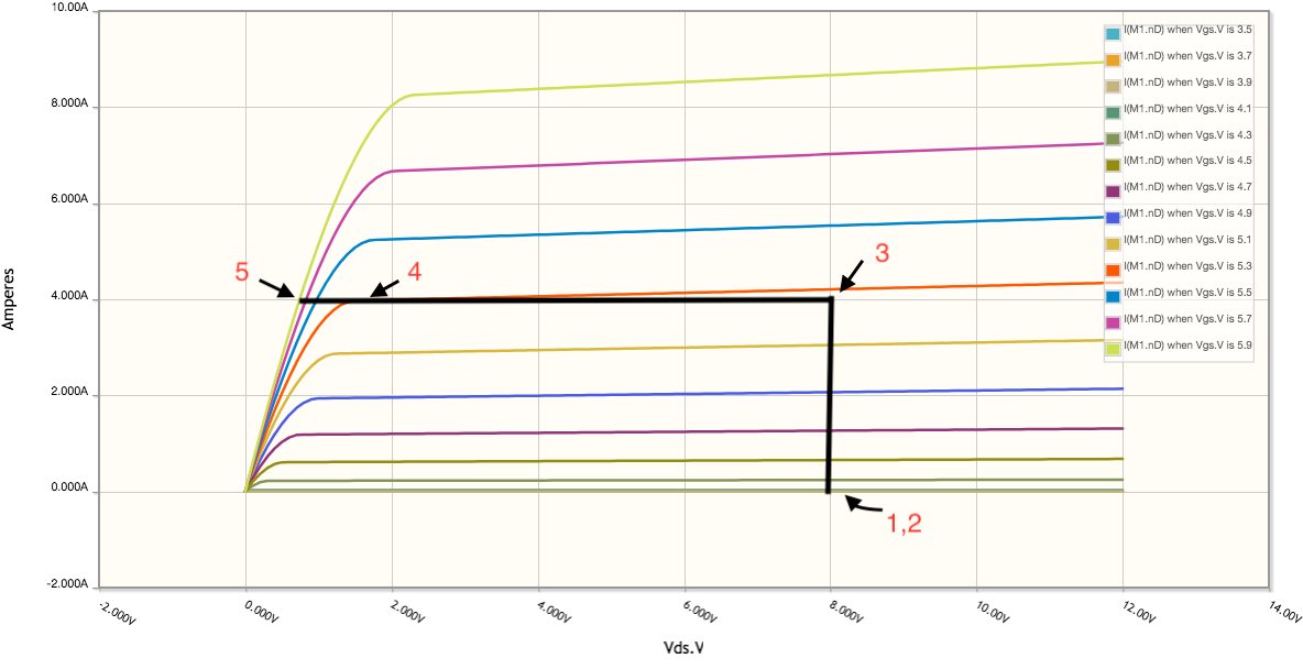
Here are the \$I_D - V_{DS}\$ characteristics given by CircuitLab's model of the IRF530. The IRF530 obviously operates with \$V_{DS}\$ well above 12V. However, to keep the plots in nice proportions, I have limited the graph to 12V.

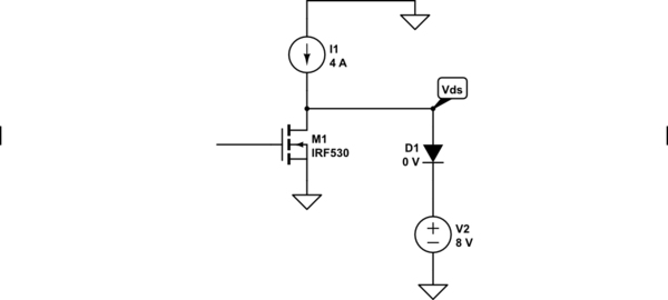
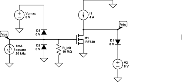
Let's place the MOSFET into a circuit with the following constraint.
- Either \$V_{DS}=8 V\$ or \$I_D = 4 A\$

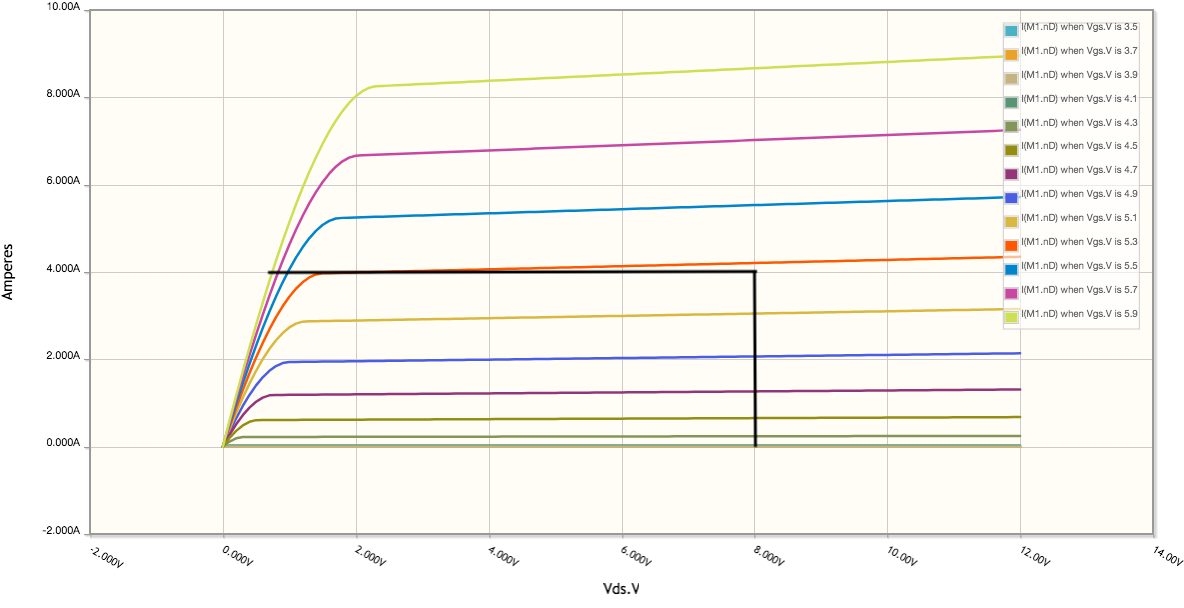
When the MOSFET is placed in such a circuit, where either \$V_{DS}\ = 8V\$, or \$I_D=4A\$, then the \$V_{DS}, I_D\$ point will lie on one of the two black lines at 8V and 4A in the following diagram.

It is important to note that, in the case under consideration,
- Any \$(V_{DS}, I_D)\$ operating point will lie on one of the two black lines at 8V and 4A in the above diagram diagram no matter how much or how little charge is present in the MOSFET gate!
Now lets consider what happens when we add circuitry that changes the charge in the gate. In this example, we are only applying 1mA current to the gate. This might be 3 orders of magnitude smaller than what one might see in practice. We use such a small current because it makes voltage drops across parasitic impedances negligible.

simulate this circuit – Schematic created using CircuitLab
We show \$V_{DS}\$, \$I_D\$, and \$V_{GS}\$, and we annotate 5 particular points of interest.


Point 1 is where \$V_{GS}=0 V\$. At this point, \$I_D = 0\$ and \$V_{DS}=8V\$. The MOSFET is in cutoff.
Point 2 is where \$V_{GS}=V_{Th}\$, the threshold voltage. \$I_D\$ is still 0, and \$V_{DS}\$ is still 8V. The MOSFET is entering saturation.
At point 3, \$I_D\$ has reached its maximum value determined by the external circuit. The external circuit enters a constant current regime, and the Miller plateau begins. The MOSFET is still in saturation. \$I_D=4 A\$ and \$V_{GS}\$ is still at 8 V, but what is \$V_{GS}\$? We will find out shortly.
Point 4 is where the Miller plateau ends. The MOSFET is on the border of saturation and the Ohmic region. \$I_D=4 A\$ because we are still in the constant current regime. What is \$V_{DS}\$? Why is \$V_{GS}\$ the same, or at least approximately the same as in point 4? Again, we will find out shortly.
Point 5 is where \$V_{GS}\$ reaches the maximum value allowed by the gate drive circuit. (In this case 8 V.) \$I_D\$ is still 4 A, because we are still in the constant current regime. What is \$V_{DS}\$?
To answer these questions, we map each \$V_{GS},I_D\$ point onto the \$V_{GS}\$ vs \$I_D\$ characteristics curve.

We see from this plot, that point 3, the start of the Miller plateau in this circuit occurs, when \$V_{gs}\$ is slightly below 5.3 V. We also see that the end of the Miller plateau, at point 4, is about 5.3 V.
It should be clear from this diagram that
- The Miller plateau is flat and level in this circuit because the Miller plateau occurs when the drain current is kept constant and the MOSFET is in the saturation region. From the \$V_{DS}\$ vs \$I_D\$ characteristics, when the drain current is kept constant and the MOSFET is in the saturation region, then \$V_{gs}\$ can vary only slightly.
It should also be clear that
- The voltage at which the Miller plateau begins in this circuit is \$V_{GS}\$ corresponding to the point where the constant current regime of \$I_D\$ begins. We do not need to know what the charge in the gate is.
And to reiterate one more time
- When a MOSFET is operated such that its drain is under a constant-voltage-constant-current regime, any \$(V_{DS}, I_D)\$ operating point for the MOSFET will lie on either the constant voltage line or the constant current line, no matter how much or how little charge is present in the MOSFET gate!
There is one more question that we hoped to answer with the \$V_{DS}\$ vs \$I_D\$ characteristics plot. That is, what is \$V_{DS}\$ at point 5? To answer that question, we follow the curve for \$V_{GS} = 8 V\$ (its maximum value) until we intersect the line \$I_D = 8 A\$. The intersection point is about \$V_{DS}\approx 0.8V\$.
There is more that can be said about Miller plateaux, for MOSFETs in different circuits, (such as the use of a drain resistor, instead of a current limiter), or different circuit parameters (such as high gate currents which cause voltage drops in parasitic impedances). But for the moment, this answer seems long enough.

