1
\$\begingroup\$

I am trying to understand the mosfet turn on procedure. This is from the following application note by TI. https://www.ti.com/lit/ml/slua618a/slua618a.pdf?ts=1613979703351&ref_url=https%253A%252F%252Fwww.google.si%252F

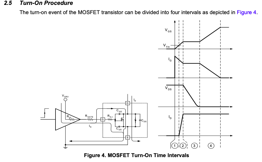
I can't seem to get my head around certain aspects of the description. In stage 2, the VDS stays constant. The rationale for this in the application note is as follows:

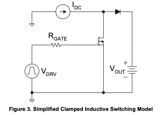
This can be understood looking at the schematic in Figure 3. Until all the current is transferred into the MOSFET and the diode is turned-off completely to be able to block reverse voltage across its pn junction, the drain voltage must stay at the output voltage level.

What is this battery voltage source? Does the diode basically turn off once all the current (from IDC and battery flow through the FET?) and that's when the VDS starts to drop?

The second aspect is around the drain current now staying constant in stage 3. The description for this is:

All the gate current available from the driver is diverted to discharge the CGD capacitor to facilitate the rapid voltage change across the drain-to-source terminals. The drain current of the device stays constant since it is now limited by the external circuitry, that is, the DC current source

The CGD capacitor is discharging current due to the rapid dv/dt on the drain terminal. This current would it not flow through the drain terminal? Would that not raise the drain current? Why is it limited to the external circuitry now?

I know from the mofet transfer curve, this behaviour happens once the mosefet reaches the saturation region, the current is roughly constant for a given gate voltage but why does that happen whilst the Vds is falling?

I think i might be confusing my concepts, so any alternative explanation to what has been provided in the TI note might just help this click. So thank you for the patience to read through this.

enter image description here

enter image description here

\$\endgroup\$
1

1 Answer 1

2
\$\begingroup\$

Vout is represented as a battery because it's such a relatively large capacitance that you can't effect its voltage. It could just as well be a very large capacitor at the time scales they are considering but for simplicity, they want you to ignore any possible charge-discharge characteristics of capacitors on the output. While the device is in the off state, all current from Idc is charging the battery but since it's such a high capacity, the voltage doesn't change so Vds is the battery voltage plus the Vf of the diode. As the gate reaches Vth the current in the device starts to increase and the current charging the battery decreases proportionally which means that Vds remains the same. Once the current of Idc is fully flowing through the device, the Vds drops below Vout+Vf and the diode turns off. It think it would be very useful if Rds and Rbat+Rdiode were included in that graph. It would make some things easier to visualize.

In stage 3, the drain current stays the same because of the inductive current source. Remember that the collapse of the magnetic field has the effect of trying to keep the current steady (at short time scales). Cgd is relatively small, so the charging current can be neglected in light of the much larger Ids. Vds is falling at his point because Rds is falling but the Ids remains constant.

Edit: During stage 3, the Miller plateau (on Vgs) is caused by the change in Vds being coupled through the Cgd which keeps the voltage on the gate from increasing at the same rate as it did in stage 1 & 2 even though it continues to charge. In stage 4, the Vgs continues to rise after Vds approaches it's minimum. Vgs in stage 4 typically looks more like a capacitor charging than a linear slope but for illustration purposes, I think it's okay.

There is a nice explanation of Miller plateau here

\$\endgroup\$
4
  • \$\begingroup\$ Thank you most of it makes sense now! In stage 3, all the Id is flowing through FET, diode is reverse biased, and Vgs is constant. So why is the Rds on still falling? I would have thought it should fall as Vgs rises and the channel opens up more. Once the channel is fully open (or not being opened further) the rds on would stay constant? Could you elaborate on that alittle? (Intuitively vds drop makes sense, the FET is on and VS is at gnd, VD is at Id * Rdson and so VDS is small. \$\endgroup\$
    – Hasman404
    Commented Feb 24, 2021 at 7:13
  • \$\begingroup\$ @Hasman404 I made an edit to clarify the Miller plateau. Let me know if that helps. \$\endgroup\$ Commented Feb 24, 2021 at 15:03
  • \$\begingroup\$ I've fallen for another confusion here. The stage 2 where the Vg goes from VTh to V miller, we say that the op amp is in it's linear region of operation as Id is proportional to Vgs. However Vds is at Vdsoff which is a big voltage. I thought for fet to be in linear VDS had to be very small. Could you explain that too please? \$\endgroup\$
    – Hasman404
    Commented Feb 26, 2021 at 8:14
  • \$\begingroup\$ Vds is being "regulated" by the diode and battery. This means that the voltage must be equal to Vbat + Diode Vf until the diode switches off once all the current from the inductive current source can flow through the MOSFET. \$\endgroup\$ Commented Feb 26, 2021 at 10:01

Your Answer

By clicking “Post Your Answer”, you agree to our terms of service and acknowledge you have read our privacy policy.

Not the answer you're looking for? Browse other questions tagged or ask your own question.