0
\$\begingroup\$

I am doing a PCB layout with a Atmel/Microchip MCU ATSAML21E18B-MUT‎ which has QFN-32 package 5x5 mm. This board can have a maximum of 20x40 mm and I am having problems with space because the circuit is not very little and also there is an NFC antenna on-board that occupies 14x14 mm on both sides.

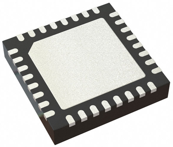
The drawing of "32 pin QFN" is on page 1123. The datasheet does not mention if this pad should or not be connected to GND or other signal.

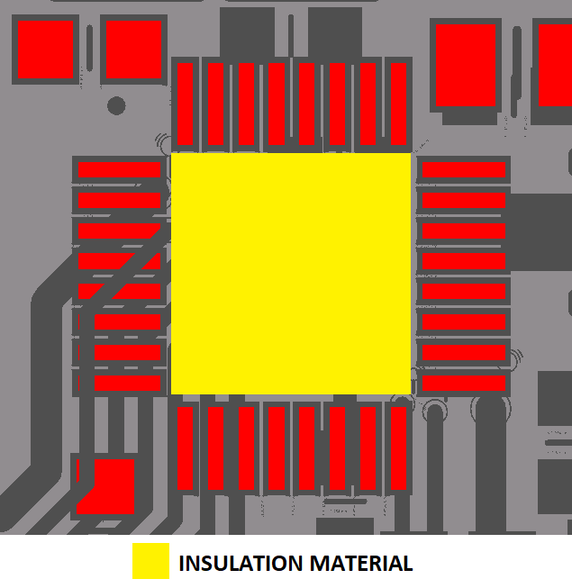
Check my current drawing of QFN-32 package on the current layout below, there is a 2.8x2.8 mm square pad in the center, also known as an exposed pad. I want to delete it... in order I can route tracks and vias below the QFN package. Doing this I would finish the layout easily.

enter image description here

And, when assembling the boards, I want to place an electrical insulation material between the IC package and the board, to guarantee there will be no short-circuit between the center pad of the QFN-32 package and a via or track, for example, if the solder mask doesn't guarantee it.

enter image description here

Then, in this case, can I securely remove the center pad of the QFN-32 from the PCB layout?

  • OBS1: It is a double-side board, there is no possibility to go multilayer.
  • OBS2: The IC does not heat.

The package:

enter image description here

\$\endgroup\$
4
  • 1
    \$\begingroup\$ "place an isolating material": you realize that's exactly what solder mask is, right? \$\endgroup\$ Commented Mar 8, 2020 at 14:59
  • \$\begingroup\$ Yes, I know solder mask is an insulator, but maybe its isolation could not de 100% perfect considering the production of a high quantity of boards and a possible imperfection on the PCB fabrication. That would be just to have a guarantee. \$\endgroup\$
    – abomin3v3l
    Commented Mar 8, 2020 at 15:09
  • 1
    \$\begingroup\$ pretty weak argument: if your boards are so cheap that you have to pay for the extra almost certainly manual step of putting an insulator below a QFN device (however you'll guarantee good soldering after), then maybe get better boards made. \$\endgroup\$ Commented Mar 8, 2020 at 15:16
  • 2
    \$\begingroup\$ Why can't you go multilayer? If it's because of cost, your solution is almost certainly worse than the problem you're trying to solve. \$\endgroup\$
    – The Photon
    Commented Mar 8, 2020 at 18:06

1 Answer 1

4
\$\begingroup\$

My conclusion upfront: It's not worth considering going your route, the potential downsides outweigh the fact that you might get a more compact layout.

Generally, you'd have to triple-check that your device doesn't run too hot with the thermal pad unconnected. So, you'd have to use the datasheet (thermal resistances) and a power model of your IC to estimate how much electrical power gets converted to thermal energy in your actual application, and estimate whether the die-to-top-of-package || die-to-contacts thermal resistance is low enough for the device to stay cold enough. Then you'd have something that probably works.

I'd have a slightly queasy feeling about that. Microchip added that thermal pad to the package for a reason.

Also, let's talk layout here:

With your trace width, you can only route 1 top-layer trace between the pads on the corners; so, no need for more clearance on the top layer than you already have. Bottom layer: you have a lot more freedom. You'd want to connect a large ground plane to the top layer thermal land through a couple of vias, but nothing's forcing you to make that cover the whole bottom of the IC package.

Anyway, what you've drawn as bottom layout doesn't look OK to me. Decoupling caps don't help much if the ground current path is worse than the Vcc path! So, your layout looks questionable on more than the thermal side of things.

So, re-layout the whole thing, starting with the attempt to put as little as possible on the bottom layer – and if possible at all, have one large, uncut ground plane. Yes, that will bump all our bottom-side components to the top side. But please believe me, during assembly (or, when paying someone to assemble), you'll be happy when you've eradicated the need to solder SMD on two sides.

One more thing: make sure your top-side capacitors are out of the keepout zones of the QFN package. What you've placed looks unncessarily hard to solder.

Generally: If this is one of the first designs you do, start with a board with four times the space you'd love to use in the end, and lay it out completely, following best-practice rules of keeping the ground plane clean, arranging passives in groups that are easy to assemble/solder, including enough test points, having really enough decoupling caps, and so on. If your finished design then really looks like you can shrink it down in both dimensions by one half, do that. Don't start with "I need to squeeze this down to the smallest possible area"; that almost always goes wrong (believe me, that's how I lost my first couple of boards).


\$\endgroup\$
5
  • \$\begingroup\$ Well noted. I yet have the doubt if the exposed pad can be left floating or if it needs to be connected to GND. \$\endgroup\$
    – abomin3v3l
    Commented Mar 8, 2020 at 15:30
  • 2
    \$\begingroup\$ The datasheet thermal resistance almost certainly assumes the thermal pad is used. \$\endgroup\$
    – The Photon
    Commented Mar 8, 2020 at 18:07
  • \$\begingroup\$ @ThePhoton For example, in a past project I did used an analog switch IC, part number FSA2567MPX, package "16-WFQFN Exposed Pad". I have left the exposed pad floating on the PCB layout, and the project worked well. \$\endgroup\$
    – abomin3v3l
    Commented Mar 8, 2020 at 19:28
  • 1
    \$\begingroup\$ @abomin3v3l sorry, but that doesn't mean the thermal resistance in the datasheet assumed no thermal pad connection. A microcontroller could easily be low enough power not to need the thermal pad, but it's going to be difficult to prove it from information in the datasheet. \$\endgroup\$
    – The Photon
    Commented Mar 8, 2020 at 19:35
  • \$\begingroup\$ @ThePhoton Thanks for help! I already have a prototype of the current circuit (with greater dimensions), and I can afirm the microcontroller does not heat anything, it runs 'cold' with package temperature very close to the ambient temperature. And now I will try to make a smaller layout. I will try dual layer PCB without the pad on the layout. Actually I will draw a very small pad in case it be necessary to connect the exposed pad to GND, but a very small one, not 2.8x2.8mm complete size... \$\endgroup\$
    – abomin3v3l
    Commented Mar 8, 2020 at 20:00

Your Answer

By clicking “Post Your Answer”, you agree to our terms of service and acknowledge you have read our privacy policy.

Not the answer you're looking for? Browse other questions tagged or ask your own question.