I am designing a JTAG Controller using verilog. Now my question is :
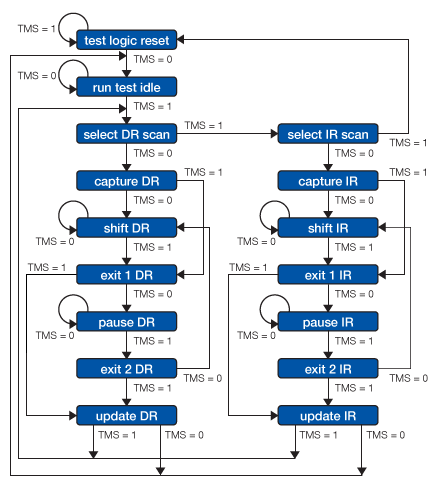
As per the state diagram of JTAG IEEE standard, in the below diagram 
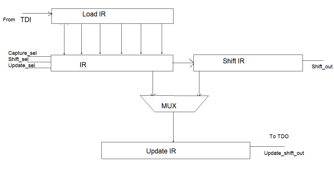
The Instruction /Data is loaded from a parallel register in Capture IR/DR state. The it can either go to shift IR/DR state or directly go to exit 1 IR/DR state if it need not shift. Finally, the FSM has to reach update IR/DR state after which a new instruction/data will be sampled. Till this point I understand, for which I have thought of a design as shown
As per my understanding, when the path selected in FSM is Capture IR-->Exit 1 IR-->Update IR, then the Load IR register will load data onto IR register when Capture_sel (from TAP Controller) is high.And IR will update to Update IR register when Update_sel is high. Other option being, after Capture IR state, next is Shift IR state, such that data loaded into IR register from Load IR is shifted serially into the Shift IR register every cycle of TCK. Finally both the paths reach update IR state, hence the IR value will be loaded into the Update IR from either IR register or Shift IR register depending upon which path taken from Capture IR state. Finally, data will be shifted out of Update IR state into TDO.
I want to know if my understanding is correct.
I also read that the TDO is driven Z (high impedance) when the state in not Shift IR/Shift DR which should mean that data is shifted out at Shift IR state and not wait for Update IR state to shift out. Which of these interpretations is correct?
If data is shifted out at Shift state, what is the need of Update state? Also, when the path taken is Capture IR-->Exit 1 IR-->Update IR, then it bypasses Shift IR state. Does that mean IR is not shifted out? What is the intention of doing so?


