2
\$\begingroup\$

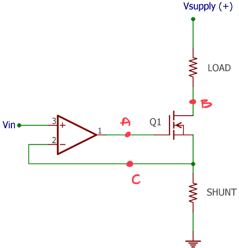
I am trying to analyse the voltages in a voltage-controlled current source.

What I have so far:

  • Vin = V_C
  • V_B = Vsupply - I_shunt*R_load

However, I don’t know how to find an equation for the op amp’s output voltage at the gate of the FET (V_A).

Could you please help explain/show how I’d be able to find the voltage at node A? I am really stuck since I don’t know how to find the the output voltage of an op amp when a relationship between the input and output voltage can’t be found using nodal analysis.

Any help would be greatly appreciated!

enter image description here

\$\endgroup\$
7
  • 4
    \$\begingroup\$ You can't from the information provided. You'll need the graphs from the datasheet. \$\endgroup\$
    – Transistor
    Commented Jul 27, 2021 at 15:58
  • 1
    \$\begingroup\$ Are you trying to do a small-signal or a large-signal analysis? A small-signal analysis may be sufficient for certain goals, such as analyzing the stability and frequency response in a narrow operating range, and can be made simpler by replacing the MOSFET with a simple linear model. \$\endgroup\$
    – nanofarad
    Commented Jul 27, 2021 at 15:58
  • \$\begingroup\$ @nanofarad honestly I was doing neither. I thought that the op amp’s output voltage is independant of the FET’s behaviour since the op amp’s inputs are independent of the FET and I am assuming Vin is DC. Is that valid reasoning on my part? How should I approach the problem? Thank you! \$\endgroup\$
    – Aeon
    Commented Jul 27, 2021 at 17:17
  • \$\begingroup\$ @Aeon the voltage is not independent of the FET because of feedback. The FET input affects the shunt voltage which feeds back to the op amp. Depending on the speed of various components this either settles to a stable value, or causes oscillations. \$\endgroup\$
    – nanofarad
    Commented Jul 27, 2021 at 17:19
  • 1
    \$\begingroup\$ Ah okay, thank you very much! \$\endgroup\$
    – Aeon
    Commented Jul 27, 2021 at 17:20

2 Answers 2

5
\$\begingroup\$

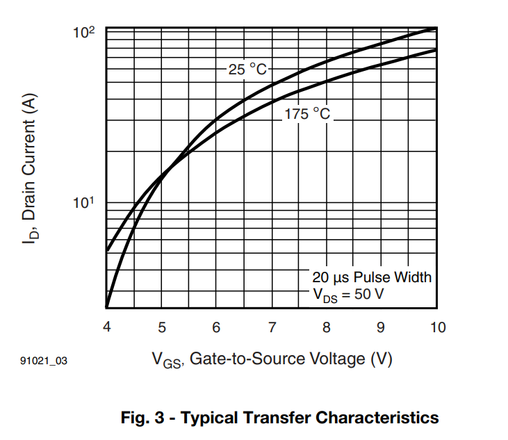
You need the MOSFET characteristics. For example, the IRF540 has the following typical characteristics:
enter image description here

So, for example, if your current is 10A the typical Vgs is about 4.75V. You need to add that to the voltage across the shunt to find the output voltage of the op-amp that is required to balance the op-amp.

The op-amp will attempt to drive the gate in order to balance the input voltages. If that is not possible the op-amp output will "rail" near the positive supply voltage of the op-amp for large input voltage (might be a couple volts or more below depending on the type of op-amp).

Similarly for very low input voltages the op-amp can only "rail" near the lower supply voltage. In some cases only within a few volts. If the MOSFET conducts too much with that voltage applied (either due to the non-zero Vgs applied or due to leakage) then it will not be possible for the op-amp to balance.

So to analyze a real circuit you would need both the transistor characteristics (worst-case if you're doing a serious design, 'typical' if you're just trying to make a best guess as to what will happen) and the op-amp characteristics. If you have an ideal op-amp, then only the transistor characteristics matter.

\$\endgroup\$
3
  • \$\begingroup\$ That makes a lot of sense. Thank you for the thorough explanation! \$\endgroup\$
    – Aeon
    Commented Jul 27, 2021 at 17:23
  • \$\begingroup\$ Note that this graph assumes that VDS is much greater than VGS. Your supply voltage should be well above the op-amp's output voltage. \$\endgroup\$
    – Adam Haun
    Commented Jul 27, 2021 at 17:44
  • \$\begingroup\$ @AdamHaun raises a good point. Vsupply can actually be very low or very high if you want it to be (for example, if you want to draw a large current out of a 1.2V battery as an electronic load) but 1) The op-amp must be able to produce the required Vgs (plus the shunt voltage) and 2) The voltage across the MOSFET (Vds) must not be so low that it cannot conduct the required current. So if the MOSFET can conduct 10A with 0.8V across it then your shunt voltage should not be greater than 400mV in the 1.2V battery example. The op-amp might need a 12V supply to make that happen. \$\endgroup\$ Commented Jul 27, 2021 at 17:49
4
\$\begingroup\$

Could you please help explain/show how I’d be able to find the voltage at node A?

voltage at A is whatever it takes to make Q1 turn on enough so that the voltage across the shunt (Ishunt *Rshunt) is equal to Vin. What that actually turns out to be depends on the characteristics of Q1.

\$\endgroup\$
1
  • \$\begingroup\$ Oooh okay, thank you very much! \$\endgroup\$
    – Aeon
    Commented Jul 27, 2021 at 17:21

Your Answer

By clicking “Post Your Answer”, you agree to our terms of service and acknowledge you have read our privacy policy.

Not the answer you're looking for? Browse other questions tagged or ask your own question.