3
\$\begingroup\$

We are using W25Q128JV Flash IC in conjunction with nRF52 SoC.

Datasheet of flash: https://www.winbond.com/resource-files/W25Q128JV%20RevH%2003102021%20Plus.pdf

We face following issue: SPI communication doesn't work. However if we connect logic analyzer (similar to this https://www.sparkfun.com/products/15033) to the DI, DO and CLK lines then everything works great. Thats why I'm certain that it is not software related problem.

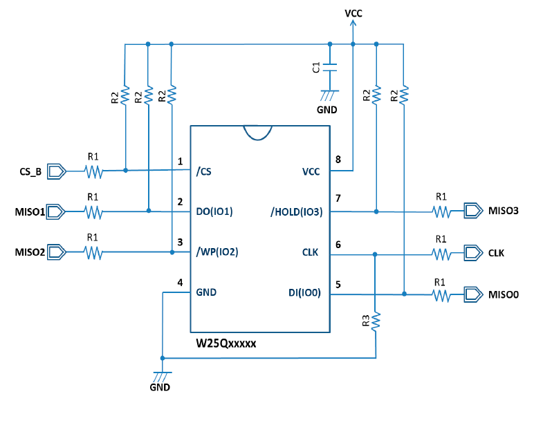
Below is schematic from the datasheet:

enter image description here

In our PCB we have following configuration:

  • R1: not used
  • R2: 10kOhm
  • R3: 100kOhm
  • C1: 0.1uF

We thought that problem is missing R1 in our design. So we added R1 to DO, DI, CS and CLK (50Ohm). It didn't help.

Also I want to note that even when logic analyzer was powered off, it still solved the communication problem.

Does anyone have idea on what is the problem?

\$\endgroup\$
5
  • \$\begingroup\$ What is talking to it? \$\endgroup\$
    – Jeroen3
    Commented Sep 8, 2021 at 12:53
  • 4
    \$\begingroup\$ A logic analyzer isn't an oscilloscope. You should actually look at the signals with a scope to see what's going on. \$\endgroup\$ Commented Sep 8, 2021 at 13:19
  • 1
    \$\begingroup\$ Are you sure the device you're talking to is properly grounded? Sometimes you can accidentally create a ground connection with bench equipment, and it's not there when the device isn't \$\endgroup\$ Commented Sep 8, 2021 at 13:21
  • \$\begingroup\$ Try putting small caps (a few pf, even ceramic disk caps will do) between lines and gnd and see what happens. See what it looks like with the scope, even if leads fix things, bad signal will still look...wel...not perfect. Do you route clock line very close to signal lines? Do you have ground plane without gaps? It can be many different things, it's just that the leads change things just enough for everything to kinda work. Nasty problem to have that's for sure \$\endgroup\$
    – Ilya
    Commented Sep 8, 2021 at 14:38
  • \$\begingroup\$ Have you checked the SPI mode? normally SPI reads on one edge and writes on the other making it reasonably tolerant of noise and mismatched delays, but if the SPI mode is wrong you may be reading and writing on the same edge. \$\endgroup\$ Commented Sep 9, 2021 at 1:43

3 Answers 3

4
\$\begingroup\$

R2 on SPI lines are not needed, WP and HOLD are different story, usually not driven by MCU.

A common value for R1 is 22 ohm, R3 isn't needed as well.

What makes yet more confusing, you call MISOx the signals that are inputs or outputs. You do have only one MISO, MOSI, CLK per SPI channel, but you could have multiple CSx, the WP, HOLD aren't part of SPI, so you shouldn't call them MISOx.

EDIT:

The resistors R1 have to be close to the source of the signal

Near MCU (MCU to Flash):

  • CS -> CS
  • MOSI -> DI
  • CLK -> CLK

Near Flash (Flash to MCU):

  • DO-> MISO
\$\endgroup\$
1
  • \$\begingroup\$ Thank you for help. It appears that MCU handles the pull-ups and pull-downs by itself with default software configuration except for MISO pin. So, in other words, when we have pull-up on MISO, and nothing else on other lines, everything worked ok. Then we reconfigured software to use pull-up for MISO as well, and now the setup works without resistors on CLK, MOSI, MISO, and CS lines. Reference: devzone.nordicsemi.com/f/nordic-q-a/53634/… \$\endgroup\$ Commented Sep 10, 2021 at 11:57
5
\$\begingroup\$

You have some noise on your signals. Where that noise is coming from is anybody's guess. But hanging the logic analyzer probe on the lines provides enough filtering of the noise that it allows things to work.

You might want to experiment with putting a LA probe on one signal at a time and see if you can narrow the problem down that way. Just guessing (a SWAG), I'd say the CLK is probably the culprit.

Note that putting 50 ohm resistors at the destination end of those signals, like you seem to have done, is not going to help. Those series termination resistors need to go as close to the source (driving end) of the signal as possible.

\$\endgroup\$
2
  • 1
    \$\begingroup\$ Decreasing the values of R2 and R3 can also help, especially if Vcc is < 5V. \$\endgroup\$
    – rdtsc
    Commented Sep 8, 2021 at 14:24
  • 1
    \$\begingroup\$ I once had a similar problem in which crosstalk between the data and clock lines was causing a tiny extra "hook" in the edge of the clock signal, advancing the state of the slave twice instead of just once per clock cycle. Took quite a while to track down! \$\endgroup\$
    – Dave Tweed
    Commented Sep 8, 2021 at 16:25
2
\$\begingroup\$

This looks like a common EMI or electromagnetic interference problem between noisy SMPS supply (s) and target. Unbalanced line impedance can also cause this due to low CMRR performance and ground path noise.

You can shunt RF noise with a cap to earth ground at supply or earth ground 0V with a wire as a 1st step. Then consider improving layout with shielding and improve common ground impedance with shielding terminated at supply end.

\$\endgroup\$

Your Answer

By clicking “Post Your Answer”, you agree to our terms of service and acknowledge you have read our privacy policy.

Not the answer you're looking for? Browse other questions tagged or ask your own question.