7
\$\begingroup\$

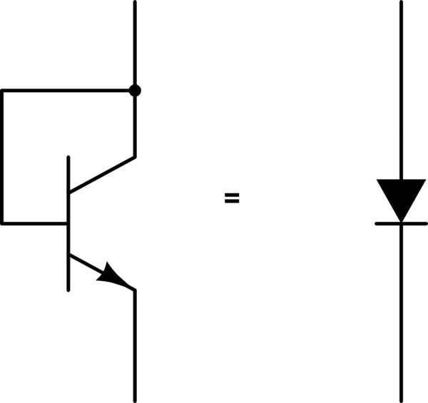
In The Art of Electronics by Horowitz-Hill, 3rd edition, in Figure 2.71, the following equivalence is shown:

schematic

simulate this circuit – Schematic created using CircuitLab

With that connection, the collector of the BJT is short-circuited to the base: base and collector are at the same potential. So, only the base-emitter junction may experience a voltage difference.

  1. Is that draw just a convention, a way to simplify the schematics, or could the BJT be perfectly replaced by a diode without variations in the circuit?

  2. Is that diode just the base-emitter diode?

  3. If the above is a perfect equivalence, does it also apply to a MOSFET?

\$\endgroup\$
2
  • 2
    \$\begingroup\$ What do the paragraphs in H&H that refer to that figure say about it? \$\endgroup\$ Commented May 4, 2023 at 14:57
  • 1
    \$\begingroup\$ @ScottSeidman Nothing, this equivalence is only shown in the mentioned Figure. It is used (IIRC) with current mirrors, in particular. \$\endgroup\$
    – BowPark
    Commented May 4, 2023 at 15:01

6 Answers 6

7
\$\begingroup\$

It is not an equivalence between a diode and a BJT, but a way to connect a BJT to be used as a diode.

Inside a BJT there are two PN junctions, both of which can act as diodes if the other is shorted out.

The BE junction, in particular, can act as a low-voltage Zener diode, because it has a max reverse voltage of about 6V or so.

NOTE: One caveat here, once the BE junction goes in reverse breakdown, the parameters of the BJT are ruined forever, especially its gain (hFE), even if you don't exceed the maximum current for the junction.

So if you want to play with a BJT connected as a diode using the BE junction as a Zener, then don't reuse the part as a BJT. Keep in mind that this is an incremental process: a single breakdown event could not alter the BJT much, but every time the current flows in reverse in the BE junction it causes a small alteration of the performance.

On the other hand the BC junction is more akin a rectifier diode, with a max reverse voltage which is the Vcb0(max) reported on the datasheet.

Your image shows the first case, where the BC junction is shorted and the BJT is used for its BE junction.

This configuration is often use as a protection diode in the signal path of small-signal electronics because it behaves as a diode with a very low capacitance, which could interfere with the signal processing if it were too big (jellybean small signal diodes that could be used have usually bigger capacitances).

Using BJTs like this has also another advantage: Bill Of Materials (BOM) optimization. If you need a low-current rectifier in your circuit that already contains a (non-specialty) BJT, you just reuse the same part connected as a diode. With modern SMD components it could even save you some board space, since a BJT in a small SOT23 package is almost as big as a jellybean 1N4148.

\$\endgroup\$
4
  • \$\begingroup\$ Not ruined forever; the decline of forward hFE with reverse bias follows a charge transport mechanism IIRC, so it takes some time to reach a failure state (hFE below specified minimum). The damage can be partially annealed out at soldering temperatures. Also note that B-C junction generally has lower leakage but higher recovery than B-E. \$\endgroup\$ Commented May 4, 2023 at 15:49
  • \$\begingroup\$ @TimWilliams Sorry, I was interrupted in the middle of an edit (real life, you know). So I was adding a note about the degradation being a gradual process. However I didn't know the damage could be reversed. Thanks for the info. \$\endgroup\$ Commented May 4, 2023 at 22:08
  • 1
    \$\begingroup\$ @TimWilliams anyway what I was trying to say is that once the BE junction breaks down, you really don't know how the specs of the BJT changed (without measuring). So, if you are learning about this thing and make some tests, it's better that you don't put back your BJT back with the other "good" ones because it may be way out of spec for other projects. \$\endgroup\$ Commented May 4, 2023 at 22:11
  • 1
    \$\begingroup\$ Degradation in Zener mode depends a great deal on the part. Old, fat, general-purpose transistors like 2N2222 don't degrade much at all. Narrow-base RF transistors are quite touchy. \$\endgroup\$
    – John Doty
    Commented May 5, 2023 at 21:42
6
\$\begingroup\$

One of the primary uses for a diode connected transistor is in temperature sensing.

In this application, the ideality factor needs to be as close to 1 as possible (as defined in the Shockley diode equation) and most diodes aren't actually that close.

Here is the venerable 1N4148

.model 1N4148   D(Is=5.84n N=1.94 Rs=.7017 Ikf=44.17m Xti=3 Eg=1.11 Cjo=.95p
 +               M=.55 Vj=.75 Fc=.5 Isr=11.07n Nr=2.088 Bv=100 Ibv=100u Tt=11.07n)

N is the ideality factor and is 1.94 so not really suitable for temperature sensing.

Now take a look at a pretty standard NPN part (where the ideality is NF (forward ideality)

.MODEL Q2n2222a npn
+IS=3.88184e-14 BF=929.846 NF=1.10496 VAF=16.5003
+IKF=0.019539 ISE=1.0168e-11 NE=1.94752 BR=48.4545
+NR=1.07004 VAR=40.538 IKR=0.19539 ISC=1.0168e-11
+NC=4 RB=0.1 IRB=0.1 RBM=0.1
+RE=0.0001 RC=0.426673 XTB=0.1 XTI=1
+EG=1.05 CJE=2.23677e-11 VJE=0.582701 MJE=0.63466
+TF=4.06711e-10 XTF=3.92912 VTF=17712.6 ITF=0.4334
+CJC=2.23943e-11 VJC=0.576146 MJC=0.632796 XCJC=1
+FC=0.170253 CJS=0 VJS=0.75 MJS=0.5
+TR=1e-07 PTF=0 KF=0 AF=1

Here it is 1.10496, much closer to ideal (there are better ones).

Transistor base emitter junctions cannot withstand much reverse voltage though (typically 6V).

NR is the reverse mode ideality factor.

You will also find diode connected transistors on the programming side of current mirrors.

\$\endgroup\$
1
4
\$\begingroup\$

The two are not entirely equivalent, because the diode-connected transistor behaves much more "ideally" than a regular diode. In the diode-connected transistor, current is divided between base and collector in the ratio 1:β, with much more current passing via the collector. This means that for any given change in total current, the base-emitter junction only experiences a tiny fraction of that change, and \$V_{BE}\$ changes by only a small amount.

The MOSFET can also be used in this way, but its "forward" voltage isn't 0.7V; that's determined by its gate-source threshold potential difference, \$V_{GS(TH)}\$. Forward voltage will therefore be subject to variation in \$V_{GS(TH)}\$ from device to device, whereas a BJT's \$V_{BE}\$ is much more predictable and similar across devices.

Also, the MOSFET has a body diode that will conduct when \$V_{DS}\$ is negative, which would not occur for a BJT with negative \$V_{CE}\$. At least not until the base-emitter junction is reverse biased enough to break down.

\$\endgroup\$
4
\$\begingroup\$

Is that draw just a convention, a way to simplify the schematics, or could the BJT be perfectly replaced by a diode without variations in the circuit?

In 2.71 where that shows up the authors are making a suggestion -- that you use diode-connected BJTs instead of using diodes because their thermal behavior will better match up with that of the output BJTs in the push-pull output stage they are discussing (assuming you mount the two of them in thermal connection with the two output BJTs shown.

You could just slap diodes in there and the circuit would still work after a fashion. But small signal diodes (in fact, almost all diodes I've experienced) have saturation currents and non-ideality emission coefficient values that deviate significantly from that of small signal BJTs.

The authors will bring up this detail not only here but in several places in different chapters moving forward.

This is one of the cases where you'll see diode-connected BJTs in practical use. Here, where the thermal behavior provides better tracking of the behavior of some other components used in the circuit and where thermal tracking is a desirable trait. Perhaps the most common use (because BJT opamps use them all over the place) is as one part of a current mirror -- the diode-connected BJT generating a voltage that is used to control another BJT's behavior and where thermal matching of some kind, once again, is not just highly desired but out-right required.

Is that diode just the base-emitter diode?

The base needs to be connected to the collector, as shown. Much of the current through the diode-connected BJT still passes by way of the collector to the emitter. It would not be the same thing to leave the collector disconnected, in case you wondered.

If the above is a perfect equivalence, does it also apply to a MOSFET?

An NFET or PFET can also be connected up like this and often is in integrated circuits where a current mirror is being constructed (for similar reasons as for BJTs, though the behavior isn't exactly the same.) So can a JFET be used like this. In fact, the authors will discuss the use of diode-connected JFETs as a protected clamp pair used in a millivolt meter (page 294) and in a peak voltage tracker (page 255.) In these two cases, because extremely low leakage is desired.

Not everything is about thermal behavior or matching up behaviors. But it often may be.

Bottom line is that there are times where a designer needs to call out the use of a diode connected active device. They will do this in the simplest way -- by drawing it up that way. That makes the suggestion explicit and clear.

\$\endgroup\$
2
\$\begingroup\$
  1. It can be replaced by a diode. It may be hard to find a diode with suitable parameters.
  2. The resulting diode can carry \$I_{Cmax} + I_{Bmax}\$. And it will be lower voltage for the same current.
  3. With an enhancement mode MOSFET with bulk connected to source, there's the body diode.
\$\endgroup\$
0
\$\begingroup\$

Short answers

Is that draw just a convention, a way to simplify the schematics...?

Yes, in circuits with many such "transistor diodes", for the sake of simplicity it is practiced to draw them as ordinary diodes.

... or could the BJT be perfectly replaced by a diode without variations in the circuit?

Yes, it could, but not "perfectly" because they are not exactly identical ("perfect equivalence" can exist between two transistor diodes or between two ordinary diodes). Usually, the idea is the opposite - to replace the diode by a BJT.

Is that diode just the base-emitter diode?

No, it is a base-emitter "diode" buffered (reinforced) by the collector-emitter part. In short, it is a "buffered base-emitter diode".

Basic idea

Understanding this as any other circuit means finding what the main idea of this connection is. The idea here is: In the circuit of an "active diode", the transistor "copies" and buffers the I-V relation of its input base-emitter junction to its output collector-emitter part. As a result, the output part becomes a "diode" like the input one.

By "diode" here is meant a voltage stabilizer, not a one-way valve (ie, the diode's property to keep the voltage constant is used, not the property to pass current in only one direction).

It is very important for the understanding of this little "mysterious" connection to bear in mind that regardless of the fact that the collector-base junction is short-circuited, the transistor works perfectly. It amplifies the base current and, as they say, "works in active mode". It does not consist of only one diode (junction) because the other is shorted; it is a transistor.

Circuit evolution

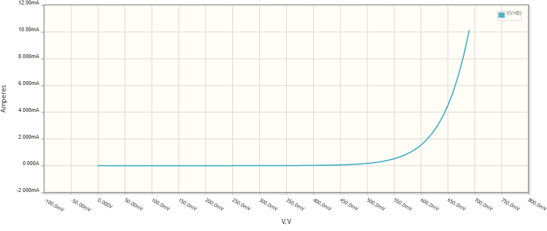
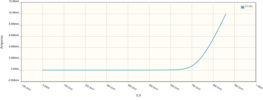
It is interesting that just two days ago I answered a similar question in detail. So I offer a shorter scenario here. It consists of a series of experiments in which the IV curves of various diodes are examined. In order to draw them in their generally accepted form (the voltage along the abscissa and the current along the ordinate), I did it with the help of a voltage source and the CircuitLab DC sweep simulation. This requires the input voltage to vary within small limits (for example, 0 ÷ 800 mV) with a very small simulation step; the output current is limited to 10 mA. So the voltage across diode changes from 0 to 800 mV and for each step, the current through diode is plotted.

Ordinary diode

Let's first examine a simple Si diode (1N4148).
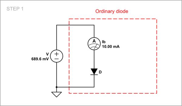
schematic

simulate this circuit – Schematic created using CircuitLab

As you can see in the graph below, in the 0 ÷ 450 mV range, the diode behaves like an ordinary constant resistor with a very high static resistance (R = V/I). After that, however, it decides for some reason to reduce its resistance. As a result, its IV curve becomes very steep (finally, almost vertical) and as they say, "its differential resistance tends to zero".
STEP 1

Base-emitter diode

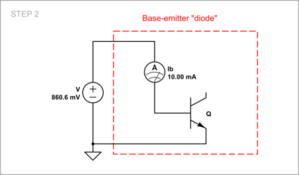
The transistor base-emitter junction behaves the same way as a diode but it seems to have a higher series base resistance B_R (10 ohm according to CircuitLab).
schematic

simulate this circuit

That is why the curve is more sloping.
STEP 2

"Current diode"

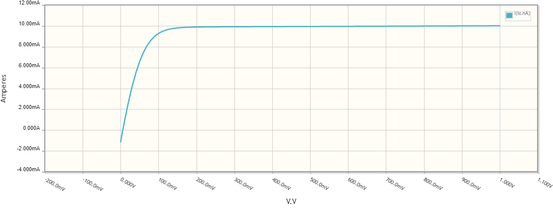
Originally the transistor acts as a transistor - keeps up the collector current constant when the base voltage is constant. Its collector-emitter part can be considered as a "current diode" (in the broad sense of the word, "diode" means a device with two ends).
schematic

simulate this circuit

As you can see in the graph below, in the 0 ÷ 150 mV range, the transistor behaves like an ordinary constant resistor with a very low static resistance (R = V/I). After that, however, for some reason it begins to increase its resistance. As a result, its IV curve becomes almost horizontal and as they say, "its differential resistance tends to infinity".
STEP 3_0

Active diode

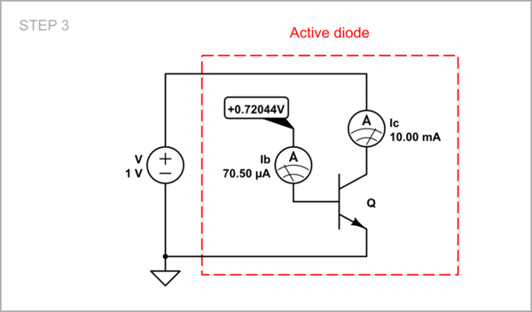
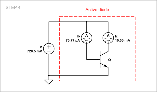
Connecting the transistor collector to its base has a drastic effect on its behavior - it begins acting as a "voltage diode" (keeps up the collector-emitter voltage constant). Its horizontal output IV curve rotates 90 degrees and becomes almost vertical. The base-emitter junction diverts only a beta part of the whole input current; so it acts as a low power (signal) diode that determines the behavior of the power collector-emitter "diode". Most of the current passes through the latter.
schematic

simulate this circuit

Since the base current is beta (140) times smaller than the collector current, the influence of the base resistance R_B on the base-emitter IV curve is insignificant and it is almost vertical (as they say, the diode differential resistance in this part is lower).
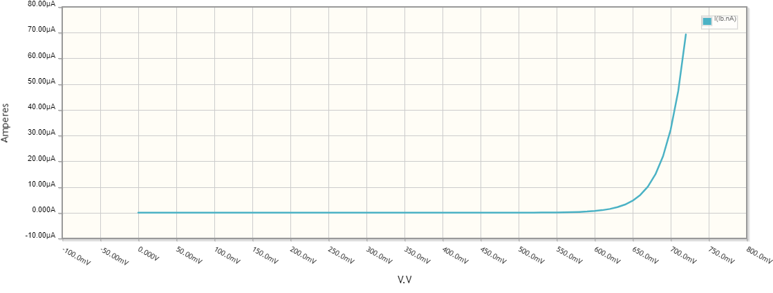
STEP 3_1

The "copy" collector-emitter IV curve is also vertical. That is why the active diode is better than the ordinary diode.
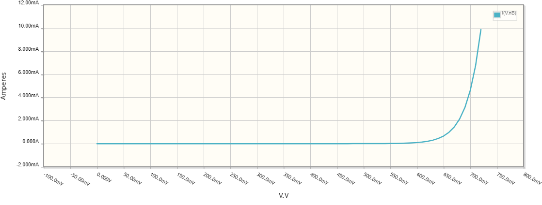
STEP 3_2

Equivalent circuit

For the purposes of intuitive understanding, we can imagine the transistor as a "current divider" of two "resistors" in parallel - a low-power dynamic Rbe and a powerful controlled Rce, which interact. I had to play around a bit to adjust their resistances to match the real transistor schematic above. As you can see, Ic/Ib = Rbe/Rce = beta (140 here); the similarity is striking.
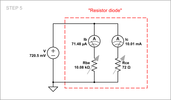
schematic

simulate this circuit

\$\endgroup\$

Your Answer

By clicking “Post Your Answer”, you agree to our terms of service and acknowledge you have read our privacy policy.

Not the answer you're looking for? Browse other questions tagged or ask your own question.