I doubt it matters.
Appnotes love to go overboard with layout instructions, but without explaining what and why; let alone giving quantitative values, or comparing alternative layouts with measurements.
Mind, so do I. It's fun to ponder layouts and optimize them to find what the limits are. The difference is, I do not fool myself into thinking I'm having a performance impact on the circuit; I do it strictly because it's fun.
So then, What is the performance impact?
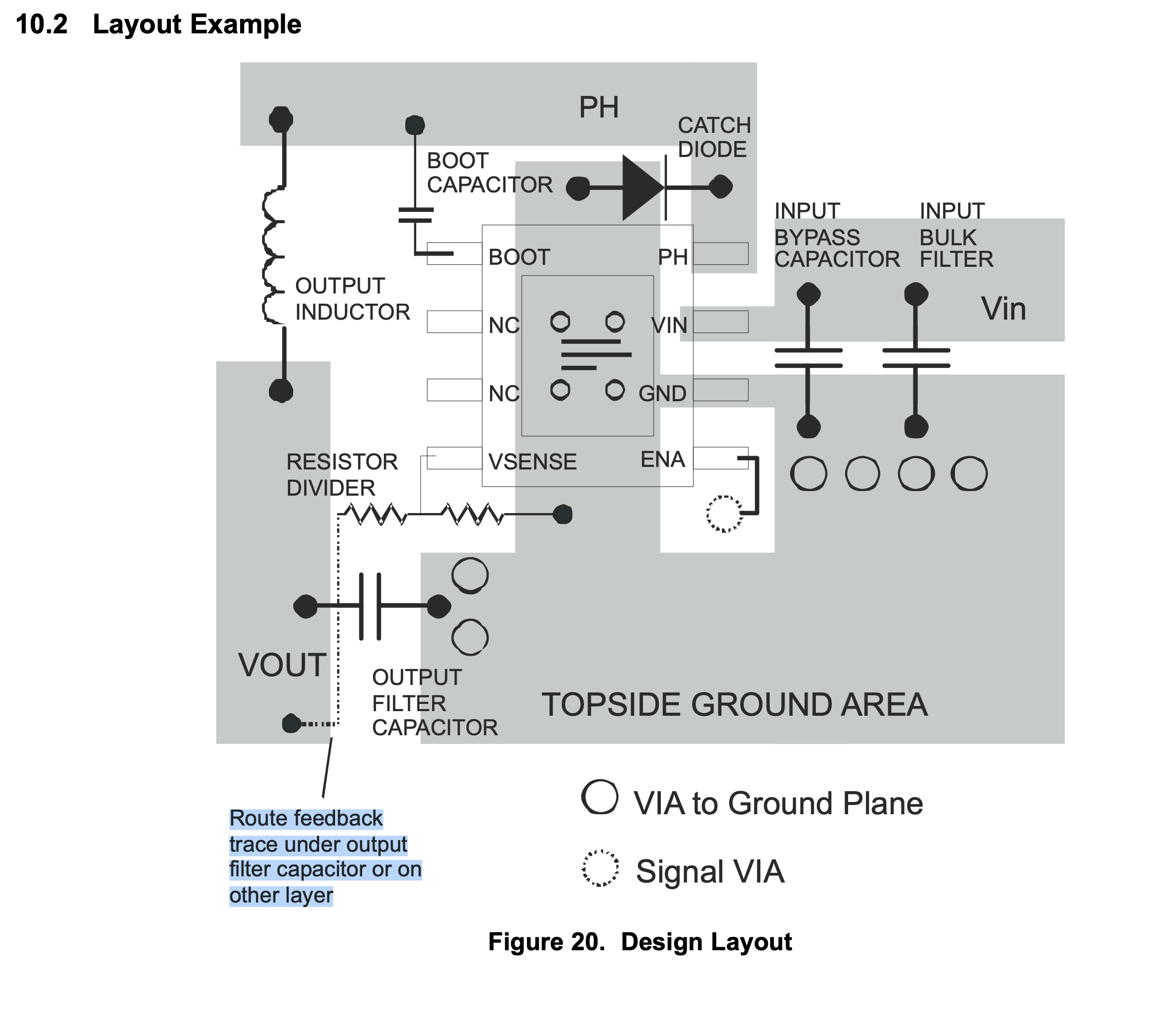
The diagram in question, indicates a connection point mere mm away from a potential closer location.
The maximum stray inductance corresponding to this routing decision is a couple nH.
This is because permeability of free space is 1.257 nH/mm. Without stopping to give proof, we can apply dimensional analysis to this constant: simply multiply by the length of trace to get its [low-frequency equivalent] inductance. There is also a geometric constant involved (typically 0.2-0.5, depending on cross-section of the trace with respect to the current return path i.e. ground plane or other nearby conductors), but we can use an overestimate (say 0.5 to 1 nH/mm) when we just want to know a worst-case sort of figure.
Thus, an extra couple nH have been added to the route.
The VOUT trace, too, has some ~nH, as does the capacitor (inductance applies to component lead and body lengths, too!), thus we have some ESL in the path between inductor, capacitor and ground.
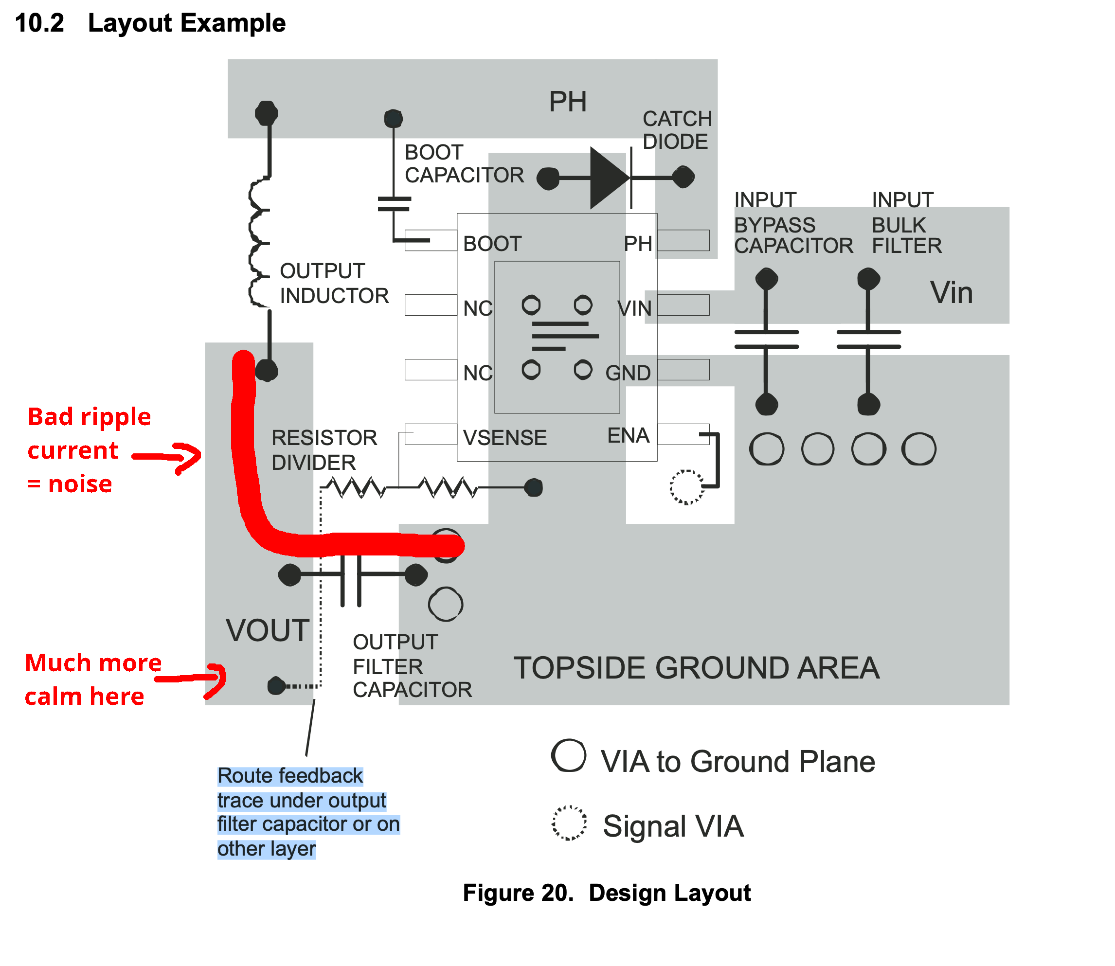
This gives us an inductor divider equivalent circuit, where the PH waveform (up to 36V p-p) drops across the filter inductor first (~10s µH), and then the ground-return inductance (including this stray inductance, and the output capacitor's; say ~10 nH total). This gives a worst-case p-p ripple purely due to switching transients alone, on the order of 36mV, at the filter inductor's VOUT pad, and perhaps 10 or 20mV further down (where only the capacitor's ESL applies).
Assuming the feedback trace has no mutual inductance to the VOUT route, the above gives the total and that's that. If not (say this is a 2-layer board), there will be some mutual inductance between these conductors, and perhaps it's closer to 25-30mV even with the distant connection point, or an improvement of maybe 5mV in that case.
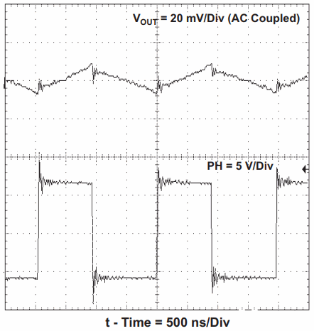
Indeed, we see partial confirmation of this analysis in the provided transient waveforms:

The output voltage ripple can be expressed as the superposition of four different waveforms:
- A quadratic (near-sinusoid; a triple-integrated square wave, with harmonics going as 1/N3) component, due to triangular inductor current ripple filtered by the output capacitance
- A triangular component, due to triangular inductor current dropping across capacitor ESR
- A square component, due to capacitor ESL acting as an inductance divider with
PH (square wave); or equivalently, the ESL acting as a differentiator against the triangular current ripple
- Random noise due to the oscilloscope, and perhaps other quirks of the system (external interference, other ringing content (particularly after the switching edges), etc.)
The noise level looks typical of a contemporary TDS460 or similar family oscilloscope, so we can ignore (4).
We're most interested in the step-like aspect, which is... probably on the order of 2mV here? Assuming the reference design, L = 15uH, and the capacitor 10TPB220M (still available today, impressive!) is 7mm long so we can expect at least 3.5nH ESL; out of 12V supply, we expect 2.8mVpp -- hey, not a bad estimate.
So what?
What difference does it make to the controller? Say we have 2.8 vs. 5.6mV applied to VSENSE, what might happen?
The controller is voltage-mode type. Its bandwidth must be a sizable fraction of Fsw, indeed below \$F_c = \frac{1}{2 \pi \sqrt{L C_\textrm{out}}}\$, and evidently a zero due to capacitor ESR is required as well (a common requirement for voltage-mode controllers). (For these reasons, we see L and Cout constrained by several relations in the given in the application section; a lossy type is also required, or an alternative circuit is given for ceramic capacitors.)
Thus, the controller will be insensitive to changes up here.
Given the block diagram, we might guess, at worst, peak noise could cause additional switching edges; but it seems likely to me, a latching driver circuit is used, so will ignore additional edges through the PWM comparator. (At that, if the error amp passes such frequencies at all.)
Due to the low bandwidth, I expect it is unlikely the controller responds to transients in this frequency range -- that is, Fsw and harmonics.
Personally, I would have no problem using a straight-line connection. My layout might end up different, anyway (due to other constraints, like nearby parts), but what they have is definitely usable. Don't worry about the dog-leg connection, just make it wherever is nearby and convenient.
Other Explanations
Maybe the diagram is not to scale. Perhaps they drew it this way, to imply that the connection should be made, indeed perhaps quite distant from the regulator, to compensate for DC voltage drop inbetween.
I don't see any reference to this offhand. And it's not like the voltage is very accurate: the tolerance of 2% is better than some, but hardly high-precision. Current isn't extreme either, at only 3A; I would gladly deal with DC resistance by simply making the layout resistance low enough not to care.
It certainly can't be connected downstream of subsequent filter components, which would incur excessive phase shift and thus oscillation. (A "zero" cap could compensate for this, like used in the ceramic cap section, but then we're changing the circuit again.)
Another possibility, is that the controller is sensitive to RF noise, and high frequencies (Fsw harmonics) should be minimized at the pin. This doesn't seem likely: the regulator is most likely of CMOS design, and the input structure is likely a CMOS op-amp that is relatively immune to RFI. But, it might also be BiCMOS, and exhibit input rectification due to a bipolar input structure. (The effect of such interference, would be to shift the voltage setpoint up or down, probably by a small amount, given we're talking single-digit mVs here.)
It seems to me, optimizing for stray inductance, without concern towards performance, is the most likely explanation. Put another way: this effort is useless, and its uselessness wasn't realized, basically because appnotes tend to be very shallow and avoid analysis.
About The Regulator
As long as I'm here, I might as well add a few nickels reviewing the part choice itself.
It's not a design win for me. I would recommend changing it to something more effective, if this is a new design. If an existing design, leave it alone.
Rationale:
Voltage-mode controls are bad. There are a variety of complex reasons for this -- some of which I've already touched on, such as compensation -- but the most prominent concern not yet mentioned, is the current limiting behavior.
The description claims some manner of per-cycle current limiting, but stops short of explaining the function, nor of how it transitions to hiccup mode. (My guess is a count of cycles terminated by peak current limiting, which is decremented or reset by "normal" (non-current-limited) pulses, and when incremented to a limit, triggers hiccup; I have seen other devices documented in this way (by TI), and it's anyone's guess why they chose not to discuss it here. Alas, this is par for the course: the general quality of TI's documentation is poor.)
It's noteworthy that the current-limiting functionality is tacked onto the control. Contrast with a peak- or average-current-mode control, where current is strictly defined by the very nature of the control itself; tolerance of startup and short-circuit conditions is natural, a given.
Now, this behavior need not be a show-stopper for any particular application; likely it works fine for 95%+ of generic power converter applications. What is a concern, is if you have an application where you did want continuous current limiting, you can't get it, there's no way to disable the hiccup function (and not that you would want to operate a "voltage mode" converter in current limit for very long anyway; they implement hiccup for good reason!). It's inflexible, and if you have a problem with these functions (maybe your design becomes heavily loaded as elements are added onto it, and it starts triggering the hiccup mode), you have little recourse but to replace the entire chip -- and thus more design work putting in a new one, choosing new components, etc.
Likewise, you have no choice over soft start (fixed ~8ms ramp time), and compensation is fixed internally.
The other aspects are general dynamics: voltage-mode controls generally perform poorly, needing overly large inductor and capacitor. Newer parts of comparable ratings might use 4.7uH and 22uF for example, ceramic capacitor is no problem, and offer comparable or better load-step response. A minor downside is, due to the higher inductor current ripple (say 30-100% of DC out), and perhaps higher Fsw, core losses may be more important; but compact, high-quality inductors are commonplace these days (for exactly this reason), so it's not hard to meet or beat the efficiency. (Not to mention, synchronous converters are readily available, doing away with the schottky's losses as well. These ratings are available in a SOT23-6 now!)
In conclusion, the most important take-away is this: traces, components, etc. (everything really, even distance itself) have inductance. We can apply hand-waved approximations to get a rough estimate (say order of magnitude or better) of stray inductance in a real layout. We can then apply expected signals to these inductances, and estimate the noise voltage due to them.
Don't loose sight of when something is worth improving, versus when it makes no further difference. Layout questions tend to be very uninteresting: most often, they either make a trivial difference, if any at all (which I expect is the case here), or such a gross difference as to be non-functional as given (e.g., ground routed circuitously on thin traces, no local bypass, etc.).
So don't worry about it. Keep the priority routes close (Cin, regulator, diode), and don't be careless with the rest (don't make a huge loop with the inductor and output capacitor, etc.). Most likely, that will be good enough, and anything additional is wasted time.
"Wasted", of course, in the strict functional sense: we can still have fun thinking about these things, and better informing our intuition about how to lay things out, for those occasions when it does matter (higher current, higher speed).


