Congratulations! The opportunity to tape out a project of your own is an exciting, although potentially intimidating opportunity (as you yourself say).
This is a going to be a pretty broad, high-level answer to give some initial background - I strongly encourage asking more specific questions based on this overview, since it definitely won't cover everything in nearly enough detail. Please add a comment if you ask a related question so I can try to add an answer, or at the very least, add links to other answers posted there. (to the OP directly, there is contact info in my profile as well)
I also can't speak to professional tapeouts, tapeouts with in-house fabs, or tapeouts on new FinFET processes. I'll be writing based on my experience taping out a 2.4 GHz RFIC on a mixed-signal 65nm process from a major commercial foundry. Almost everything I say here will have various exceptions, and I'd probably have to plaster the entire answer in footnotes to cover them all, so I'll often skip or abbreviate them.
Budgeting and floorplanning - In the world of silicon, you typically pay by the square millimeter for a rectangular chip. The area represents the space you get to design a circuit, and for the most part the perimeter represents the space you get for pins. Area can be pricy. When I taped out, a square millimeter fabricated in 65nm went for $5500 USD. We fit 47 pads (with some pad staggering). Newer processes will be costlier. Older processes might be cheaper, but might have larger minimum order sizes. Note that your department might have specific budget or grants for this, or might partner with a fab directly in some cases.
Talk to your advisor early, and try to scope what your chip will contain. Will it contain just your own circuit? Other test structures? Multiple replicas? A reference circuit so you can do an apples-to-apples comparison on the same die? Any large passives like inductors?
This is your opportunity to work with your instructor to establish your scope. Worried about the complexity/space cost/design time of on-chip transformers? Push back and propose something else. Really hoping to include a particular circuit? Make sure it's included here.
Also, skim your design rules documents. They may have rules on the size and spacing of wirebond pads, allowing you to make accurate estimates of how many pins you can afford on your chip, and generally get an initial sense of what you'll be able to do.
Cell-level schematic design - As you've mentioned, you're designing an OTA. You'll design it in schematic first, using the cells provided by your process development kit - this means that if you're using TSMC's 65nm process, you use the FETs from tsmcN65, and not some generic nfet model. You'll do your first pass on sizing, and start thinking about layout as you set the sizes - overly wide or narrow transistors would be unwieldy to lay out, and expose you to significant parasitics. It's worth giving the design rules a skim here, so you stay within any limits on transistor sizes.
The more you can "predict" your layout experience and plan ahead, the better the layout will go. Consider that you might want to take a wide transistor and split it into parallel fingers (e.g. a 40u nFET might become 4x 10u nFETs in parallel) for layout flexibility. I like to design differential circuits and I'm very particular about my transistors being well-matched, so I'll design almost every transistor to have an even number of parallel fingers, so I can build symmetric layouts later.
By this point, you should apply some circuit design theory and have a rough sense of what nets are sensitive to parasitic capacitance and resistance, which transistors need to be well-matched, etc.
You'll also make your first rounds of simulation here - in addition to standard schematic-level analyses, you'll have your first opportunity to estimate the impact of manufacturing variation. If you can, try to express your simulation using ADE XL or a similarly powerful simulation tool, with acceptance criteria (e.g. gain, noise figure, etc). Manufacturing variation can be simulated in two ways:
Corners: Each time your fab steps the wafer, implants ions, etches, etc, the result will always be a tad different. This results in effects in both the FEOL - the carrier mobilities will vary, and they'll vary separately for pFETs and nFETs - and BEOL, where the parasitic capacitance between metal layers will vary.
You can simulate at each of these corners, making sure that you meet your design goals at the typical (tt) corner and the extreme corners of the space (typically ff, fs, sf, ss). If your PDK has BEOL corners like cbest/cworst, you can run them as well. Typically, you would run the same simulations, while the simulator changes the circuit parameters slightly during the simulation.
Monte carlo: You run a large number of repeats of the simulation, drawn from the probability distribution of outcomes that the fab expects. You see how many of them pass your acceptance criteria.
Cell-level layout - This will be your first real bit of layout - you're going to take each of your elements from the schematic, and place them in real space. A lot of this is going to come down to design rules and best practices. I could spend an entire answer talking about these, so I'll list some major keywords:
- Design rules are non-negotiable. They can be checked automatically using the design rules checker and a set of rules provided by the fab. Usually the rules are provided in both a reference PDF and a set of machine-readable rules used with the design rules checker. Skim the PDF and keep it handy!
- Techniques/best practices are important for a good outcome, but automated tooling won't stop you if you violate them. Consider things like symmetry/interdigitation, abutting where appropriate, avoiding needless parasitic capacitance/resistance/inductance, ensuring that you have room to route input/output signals, good power supply layout, etc. For sensitive circuits or high frequencies, also consider crosstalk. Include guard rings where appropriate, and budget space for them.
- As you do more layout, you'll get a better sense of what works for layout, and what's prone to get you painted into a corner. Don't be afraid to rip up and backtrack if you start to get into a suboptimal situation.
- Layout-versus-schematic will reverse engineer your layout back into a netlist and check it to ensure that your layout matches your intent. This is non-negotiable as well.
- Using tools like Assura/PVS + the output of LVS, you can extract parasitics and feed them back to the simulator, to do a post-layout simulation at the cell level. Use these results to guide your layout.
- Practicing layout is a good way to get better at layout. You should seek feedback both from experts and post-simulation results to guide your work.
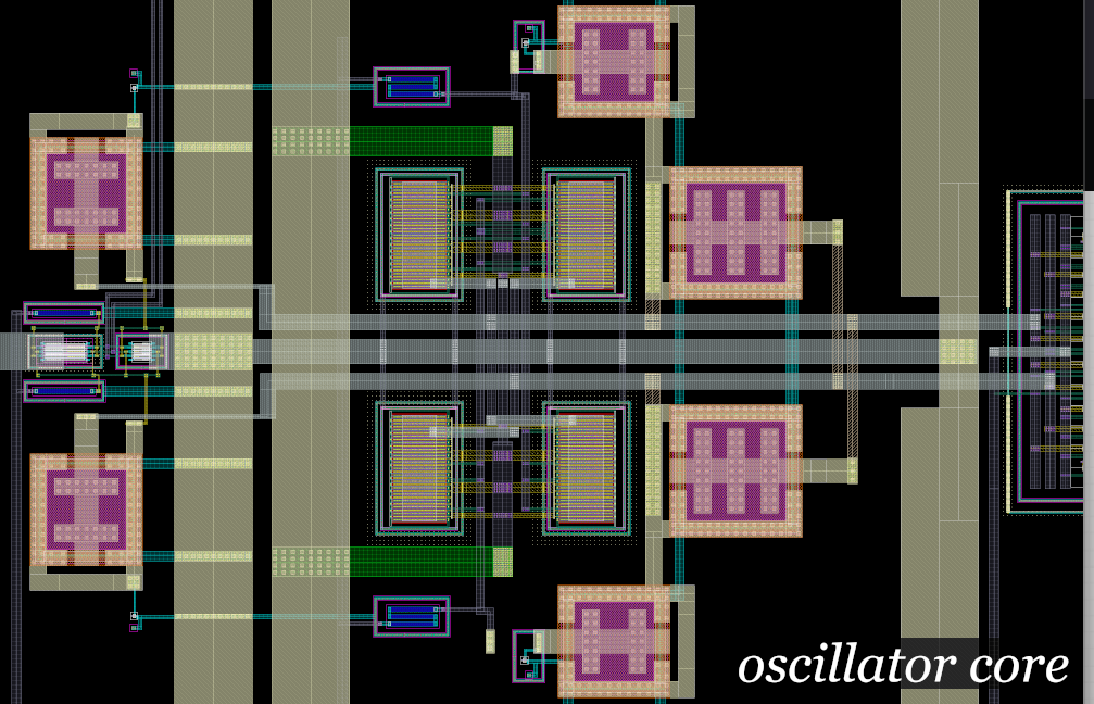
At this point, you'll have a small layout similar to this image (from my own tapeout):

Note that it's still a rather small cell, individual transistors are visible, but I've already taken some effort to get input/output signals routed to the edge of the cell. This should, on its own, pass most DRC + antenna checks (with the exception of things like density, minimum area on small connections at the edge that will be connected later, etc. For each DRC failure you accept here, you should have a plan for why it will be fixed at the full-chip phase.
Chip-level placing and routing - Once you've made all of your cells, you'll want to place them onto a full chip. Start with a schematic that reflects your design intent, including bond pads, any diodes or other structures for ESD protection, etc. Simulate that schematic.
For the layout, your design rules/PDK will have some guidance, and perhaps some templates (often in GDSII format) that you can import for common things like the edge features that all chips have. You should also have bond pads you can import from somewhere.
Here, you'll need to actually connect your cells to each other and/or the outside world. While your simulation probably ran with ideal wires in the testbench attached to ideal power supplies, you're now laying out real metal with real resistance, capacitance, and inductance. Keep electrical performance (effect of parasitics) in mind, as well as your design rules. Wide wires on high metal layers can be a good idea for power, since they'll have less parasitic impedance.
You'll want to mostly follow your floorplan from before, possibly modifying it if you discover that you're violating assumptions that you applied when making it.
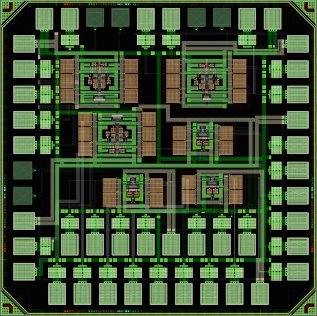
This is what the final result looks like; note that the chip has its protective edges, all cells from my floorplan are placed, pads are connected to their respective cells, power and ground are routed, etc (dummy fill should be done as well, but it's not shown in this screenshot):

If you want a personal touch, read your design rules for logos/graphics related requirements carefully, and find an empty area for a small logo or other bit of chip art. Be careful not to accidentally make it electrically active (or worse, short a power rail to the chip art or something). It's wise to leave some spacing between any art and any active circuits, especially sensitive analog circuits.
Final design rules pass - Your previous DRC applied to a single cell. Now, you have a full chip, meaning that you can validate some design rules that apply to chips as a whole. Make sure that your design rules deck is configured for a full-chip analysis, and run it. Make sure to run any packaging-specific, antenna-rules, and LVS analyses as well. You'll probably get new design rule violations. Depending on your process and tools, you might need to run a tool (or a special DRC rules deck) to generate dummy features to meet density rules; you'll need to import the result of that back into your chip. If the dummy features push you over the edge on parasitics, you might have some exclusion layers you can use to keep those features out of sensitive areas.
Again, just like most of this guide, I'm simplifying a step into a single paragraph, while it really merits its own dedicated question and answer (perhaps multiple).
Final simulations - You now have a massive design spanning your whole chip. If you needed to add metal fill, you might have hundreds of thousands, or millions, of nodes. Extract parasitics from your full chip design and run as many simulations as possible against it. Due to compute/memory limitations, you might be limited in what you can do.
As an example, in this stage I discovered that the stray capacitance of my bond pads was messing up the feedback in an oscillator that used an off-chip resonator. I couldn't run my full test suite, but simply running ac and stability analysis was enough to inform me that I needed special low-capacitance pads. I updated the schematic, layout, and determined that I now met the necessary spec.
Tape out to GDSII - You'll get a file that you can actually send to your fab. Their representative will schedule a kickoff meeting - attend it and take notes. Raise any concerns with them, and fill out any paperwork (including design rule violations you need to try to waive, chip details, etc). Be attentive to any emails or calls from them. Try to get the design in before the deadline, but don't rush if it means you'll make a sloppy error or sacrifice your well-being.
Receive chips and test - Hopefully, you've designed a circuit board to use to test your chips. Depending on how your chip is being packaged, your PCB might have to use chip on board or mount a traditional IC package. Especially if you're mounting a fine-pitch, BGA, chip-on-board, etc, talk to your board house to get recs. They might recommend a particular surface finish. Don't just use oshpark or another low-cost PCB service. Find an assembler that will be able to install the chip and any other SMT parts, and work with them to get them board layouts and pick-and-place data/fab notes.
Getting this right might be pricy. You might be doing a multi-layer, controlled impedance board with a NiPdAu finish. You might need a pick-and-place assembly house that can also do wire-bonds if you're doing chip-on-board. I think we paid on the order of $6000 USD for this assembly + some small amount for parts from digikey.
If you're doing chip-on-board, be very clear about pinout, especially if you have unusual arrangements like staggered pins (much like I do). This will be part of the fab notes package your assembler will want from you.
Document your chip - You've made a new chip and design. You'll probably get 100 or so of them because of economy of scale on foundry processes. There will be leftovers. Document the pinout, signal levels, etc - in case other students or researchers want to use leftover ones down the road. If you want, make up a fun part number or something - you have a chance to be lighthearted here in a process that otherwise must follow exacting rules. Your chip and schematic testbenches are very useful here as well.
If you like visual art, you might want to make a nice design based on your chip design - this will be a great eye-catcher for talks, thesis defense posters, etc. Grab some high-resolution views from your layout tool.
Support future students - You've gone through a very tough yet rewarding process. You've probably discovered useful tidbits of info or quirks regarding your school's software setup, your specific process, particular design rules that were hard to understand, contacts at various suppliers, etc. Create or update a wiki with information for students that will walk the path after you.
Regarding what you can do now - practice going through the layout process. Even if your OTA isn't your final design, lay it out and see how it performs. Get feedback on your layout (from classmates, advisor, this website, etc). Try techniques that seem promising, and see how they work. If you get some layout experience before designing/finalizing the schematic of your OTA, you'll probably have a better time designing for layout.
Finally, regarding knowledge and the gap - there will be a lot of knowledge to fill. That was the case for me as well - I was studying at a tiny school, under a new professor that just joined. We hadn't had a tapeout in years, and nobody quite knew what to do. My professor wanted me to tape out, I wanted to tape out. It took a lot of trial and error, some questions to Cadence, a lot of reading documentation, but ultimately we blazed that trail and got a whole cohort of students interested in doing their own tapeouts. Overall, it was an extremely rewarding process that I'd encourage exploring, in spite of the many steps and broad knowledge we had to pick up.


