0
\$\begingroup\$

I am working with an ESP32 that generates a unipolar sine wave ranging from 0V to 3.3V. However, I need to convert this signal into a true AC (Alternating Current) waveform that oscillates between +3.3V and -3.3V.

My current challenge is transforming this unipolar signal into a bipolar voltage so that it transitions into both positive and negative voltage ranges. I have researched different solutions and am particularly interested in using an Operational Amplifier (OpAmp) to achieve this.

What are the potential solutions for this conversion? How can I utilize a Rail-to-Rail OpAmp to convert the unipolar signal into a bipolar sine wave? I am looking for suggestions on the most suitable circuit to achieve this goal.

\$\endgroup\$
4
  • 1
    \$\begingroup\$ Do you have a negative supply for the OpAmp? What is the intended receiver of the bipolar signal? \$\endgroup\$
    – Jens
    Commented Sep 11 at 17:03
  • 1
    \$\begingroup\$ If you don't have/don't want a negative supply, you could possibly AC couple the signal into a small 1:2 transformer. You don't give a frequency range or drive current/load for the signal so it's hard to know if it would be a viable solution. \$\endgroup\$
    – John D
    Commented Sep 11 at 17:20
  • \$\begingroup\$ yes, I have a voltage regulator that provides a stabilized -3.3V supply. So I have a symmetrical power supply with +3.3V and -3.3V for the OpAmp.i will try it Thanks for your help! \$\endgroup\$ Commented Sep 11 at 18:45
  • \$\begingroup\$ Thank you for the explanation, and I appreciate your time. However, I thought that the circuit you created for me was simply a non-inverting operational amplifier. But now, based on your formula for 'Vout,' I’ve realized that it's actually a differential amplifier. Is that correct? The problem is that I already have a rail-to-rail operational amplifier \$\endgroup\$ Commented Sep 12 at 20:28

3 Answers 3

1
\$\begingroup\$

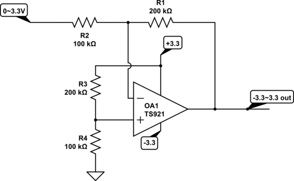
Simple way with an op-amp and dual supply rails:

schematic

simulate this circuit – Schematic created using CircuitLab

enter image description here

The op-amp has to be a RR output type that can withstand the high voltage 6.6V supply. Note that this circuit inverts.

\$\endgroup\$
1
\$\begingroup\$

Even a rail-to-rail output op-amp cannot quite get its output all the way to the rails. It will always fall a few millivolts short. Many op-amps can't handle inputs that get too close to their supply rails either. Check your op-amp's datasheet, but to be safe with most op-amps you'll need to supply the op-amp with well beyond ±3.3V.

Assuming you can do that, with say ±5V, then try this:
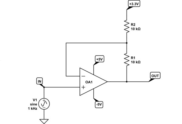
schematic

simulate this circuit – Schematic created using CircuitLab
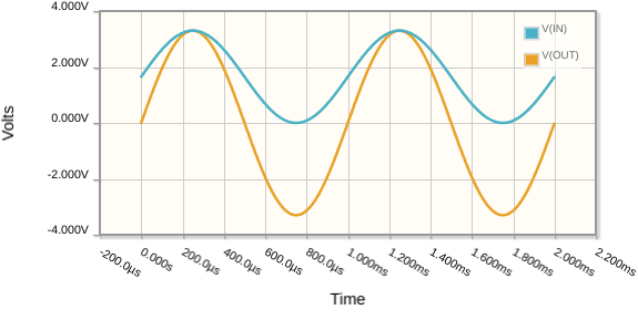
enter image description here


Update: How I derived those values.

There's a relationship between \$V_A\$, \$V_B\$ and \$V_{OUT}\$ for the following generic circuit:

schematic

simulate this circuit

The formula is:

$$ V_{OUT} = V_B\left( 1 + \frac{R_2}{R_1} \right) - V_A\frac{R_2}{R_1} $$

Find two conditions that you know to be true:

  1. \$V_{OUT} = 0V\$ when \$V_B=+1.65V\$
  2. \$V_{OUT} = +3.3V\$ when \$V_B=+3.3V\$

Plug those values into the formula to obtain two simultaneous equations:

$$ 0 = +1.65\left( 1 + \frac{R_2}{R_1} \right) - V_A\frac{R_2}{R_1} $$

$$ +3.3 = +3.3\left( 1 + \frac{R_2}{R_1} \right) - V_A\frac{R_2}{R_1} $$

Solve them to reveal two quantities, \$V_A\$ and the ratio \$\frac{R_2}{R_1}\$. Choose any two resistances in that ratio within reason. Keep them in the kilohms, for these reasons.


The word "suitable" is subjective. The above design will work fine if you're sure the power supply is stable, exactly +3.3V, and sufficiently free of noise. Any design (like the one above) that uses the power supply as a voltage reference is going to inject any offset or noise present on the supply directly into the signal.

To avoid this you'll need a precision voltage regulator, like the TL431, like this:
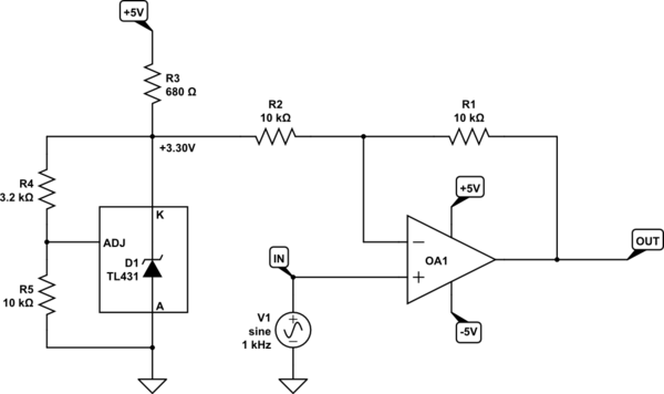
schematic

simulate this circuit

If you know the lowest frequency your DAC will ever produce, then you can get the simplicity of my first proposal and the accuracy (zero offset) of my second, using an RC high-pass filter:
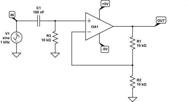
schematic

simulate this circuit

Capacitor C1 and resistor R3 are used to "AC couple" the signal. This removes any DC offset, so it becomes centered around zero volts (ground). Then all the amplifier needs to do is multiply by 2.

It has the disadvantage that the signal takes some time, about \$5C_1R_3\$ to settle at its final offset. If the lowest frequency you expect from your DAC is \$f_{MIN}\$, then you should aim for a cut-off frequency of significantly less, say by a factor of 10, \$f_C=\frac{f_{MIN}}{10}\$. Then C1 and R1 will be chosen such that:

$$ C_1R_3 = \frac{1}{2\pi f_C} $$
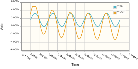
enter image description here

\$\endgroup\$
2
  • \$\begingroup\$ Thank you for your answers, they are amazing and offer a lot of options. However, I have a question: Why did you choose 3.3V at the inverting input? what role does it play? cann you explain to me the logic behind it \$\endgroup\$ Commented Sep 12 at 16:03
  • \$\begingroup\$ @Soufianebenaich I have updated my answer to show the maths, which is covered in this other answer. \$\endgroup\$ Commented Sep 12 at 18:37
0
\$\begingroup\$

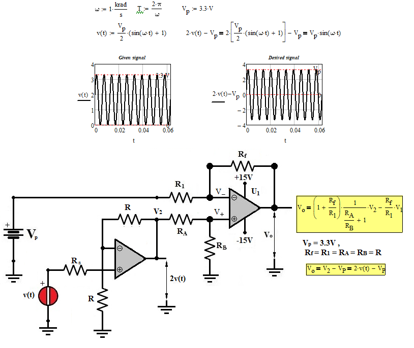
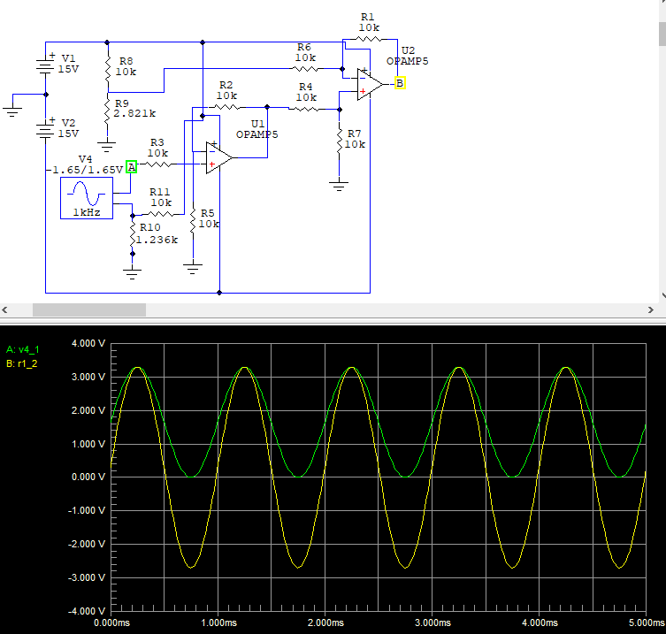
I use two Op-Amps, the first is a non-inverting amplifier with gain two. The second is a differentiator. Assuming all resistors are of equal value, the desired signal is obtained:

enter image description here enter image description here

\$\endgroup\$
1
  • \$\begingroup\$ Sounds a Great idea, thanks! \$\endgroup\$ Commented Sep 11 at 18:53

Your Answer

By clicking “Post Your Answer”, you agree to our terms of service and acknowledge you have read our privacy policy.

Not the answer you're looking for? Browse other questions tagged or ask your own question.