4
\$\begingroup\$

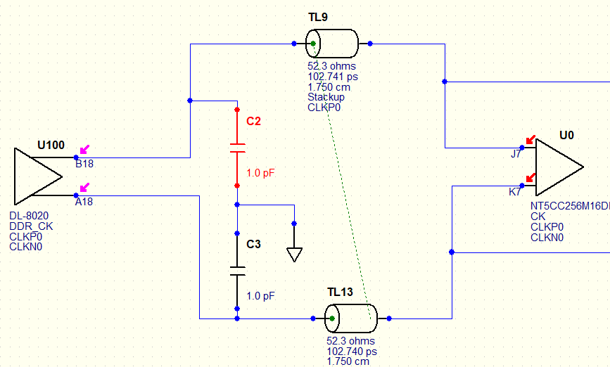
I saw in some DDR3 designs that there is a capacitor between differential clock lines, for example the image below:
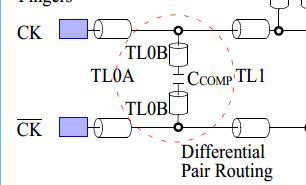
capacitor

In the document this image comes from it says:

On the DDR3 SDRAM DIMM, there is also a compensation capacitor, CCOMP of 2.2 pF, placed between the differential memory clocks to improve signal quality

My first thought was that it adds a pole at certain frequencies (problematic ones) that dampens high frequencies disturbance.

How does adding this capacitor help? I've seen some graphs and the positive effect it has (smooths the signals) but what is the (simple?) theory behind it?

\$\endgroup\$
4
  • \$\begingroup\$ Are you aware that the capacitor is connected to the main transmission line by two short transmission lines and given that your diagram doesn't specify anything about them it's difficult to determine whether the cap is acting like a cap or an inductor. \$\endgroup\$
    – Andy aka
    Commented Dec 26, 2013 at 20:33
  • \$\begingroup\$ I am aware, I dont know their lenghts. it is more of a general design question. \$\endgroup\$
    – YNWA
    Commented Dec 26, 2013 at 20:42
  • \$\begingroup\$ I think any answer will involve a bit of speculation, that's the problem I guess. I think if you look at the graph following the picture, the cap is acting like an inductor. It appears to be pre-distorting the clock signal so that subsequenct TL capacitance makes the signal on the last SDRAM still acceptable. Without the "inductor", the clock signal on the final SDRAM might be too "out-of-shape" to be usable. \$\endgroup\$
    – Andy aka
    Commented Dec 26, 2013 at 21:12
  • \$\begingroup\$ the cap' is ~1pF, and frequencies are ~1,2 Ghz, so it does adds up to an inductor. I'll go back to Transmission Line's theory books from here....thanks \$\endgroup\$
    – YNWA
    Commented Dec 27, 2013 at 16:45

2 Answers 2

1
\$\begingroup\$

This capacitor is related to jitter compensation and improving VIX threshold..

I can give few references.

  1. there is a discussion regarding this on si-list

http://www.freelists.org/post/si-list/DDR3-Clock-differential-signal-termination.

  1. www.jpier.org/PIER/pier121/04.11080302.pdf‎ "the timing jitter can be reduced by placing a capacitor to compensate for the velocity difference caused by different propagation modes"

Altera mentioned Ccomp should be added to increase the signal quality

For DDR, there are few app notes from micron and freescale which will demonstrate the compemsated Bus topology to improve timing margins. TN-46-07

I didn't find any SI waveforms which will demonstrate with or without Ccomp differences.

\$\endgroup\$
5
  • \$\begingroup\$ hi, they are talking about a shunted capacitor to ground, I was talking about a capacitor placed between the differntial clock signals. (the capacitors sizes are different also, ~uF vs. ~pF) \$\endgroup\$
    – YNWA
    Commented Dec 28, 2013 at 8:38
  • \$\begingroup\$ Shunted Capacitor is mentioned in DDR app notes..it is mentioned for single ended signals.for differential signals like DDR3 Clock capacitor will be connected parallel to CK- and CK+. It mainly recommneded when loading is more. we have used them when we are using 9 x8 DDR3 chips for each DDR3 controller. AN520 from Altera is having few words on this. \$\endgroup\$
    – user19579
    Commented Dec 30, 2013 at 6:00
  • \$\begingroup\$ Hi :) what do you mean by "when loading is more" ? \$\endgroup\$
    – YNWA
    Commented Jan 1, 2014 at 10:42
  • \$\begingroup\$ if perfect answer is required, This should be decided by simulation. We have used this Ccomp for 9 loads (x8). \$\endgroup\$
    – user19579
    Commented Jan 1, 2014 at 12:59
  • \$\begingroup\$ I think loading more means that the fanout of the clock pin is high. \$\endgroup\$
    – ajs410
    Commented Mar 28, 2014 at 18:55
0
\$\begingroup\$

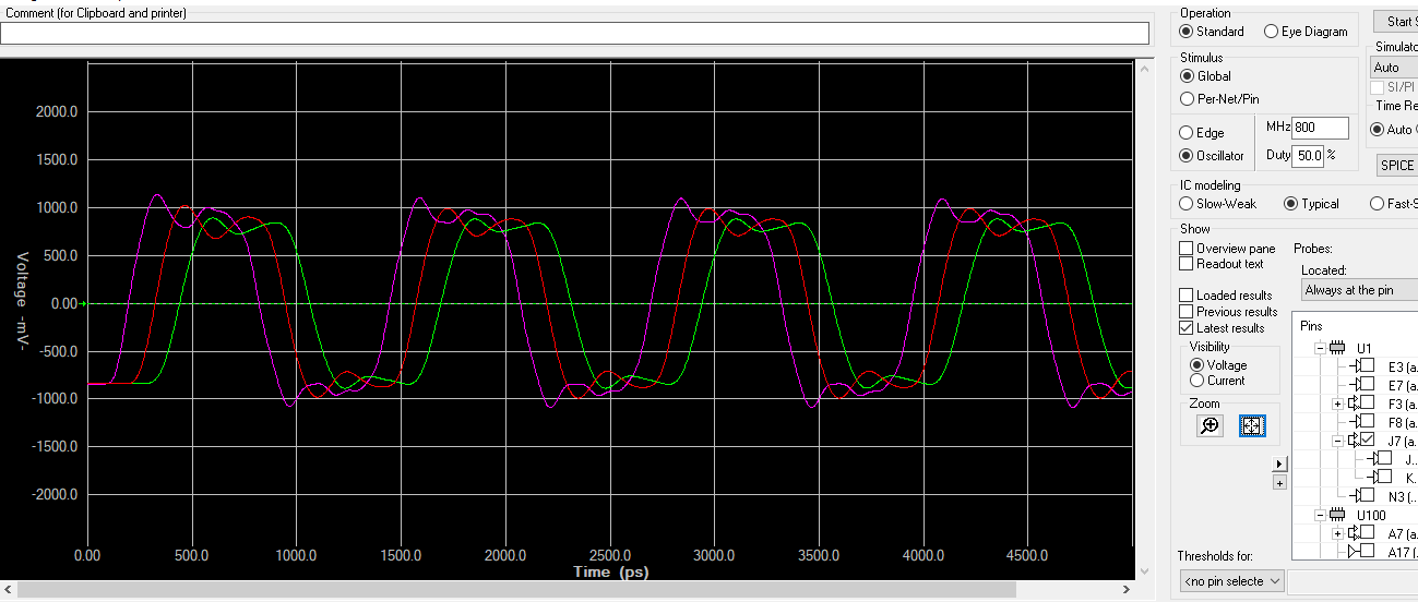
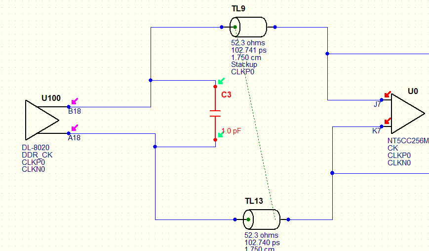
The Ccomp acts as a high freq filter. Since it's a differential trace, there's sort of a virtual ground that's not shown by the schematic. It's easier when you visualize it as two Caps connected to ground in the middle. Sort of virtual ground

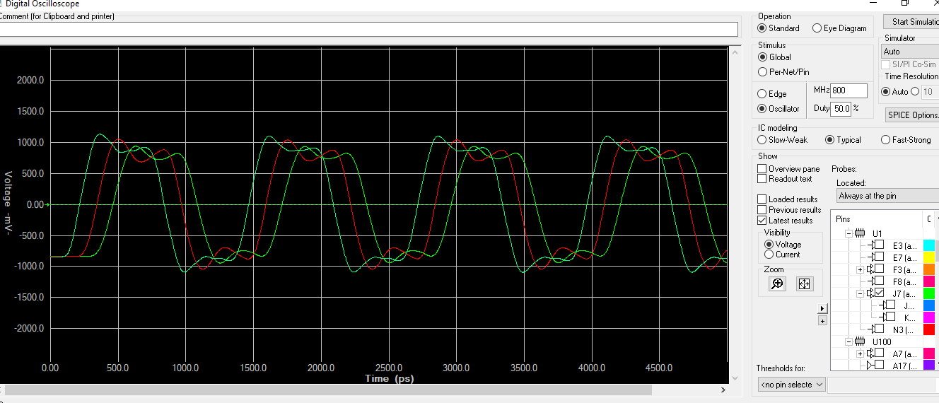
And the simulation: enter image description here

Then see similar results circuit 2 and sim 2:

Circuit1 Sim2

\$\endgroup\$
1
  • \$\begingroup\$ This is a little simplistic of an answer when Transmission Theory is known by @YNWA. It is very possible that this capacitor is acting as an inductor or as part of a matching circuit that would take too much board space to do using tuning stubs. If I recall, those blue wire will be treated as "perfect wires" and ignore the transmission theory required to solve this problem. \$\endgroup\$
    – Dave
    Commented Dec 8, 2017 at 11:30

Your Answer

By clicking “Post Your Answer”, you agree to our terms of service and acknowledge you have read our privacy policy.

Not the answer you're looking for? Browse other questions tagged or ask your own question.