1
\$\begingroup\$

I'm trying to build a voltage-controlled current source which is supposed to work with a wide range of load resistances. Currently the plan is to use an NPN transisitor as voltage follower to do the heavy lifting, and control the current with an op amp:
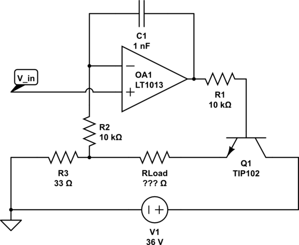
schematic

simulate this circuit – Schematic created using CircuitLab

The load resistance RLoad does not change quickly (< 1 Hz), but can vary over a huge range (10 Ohm - 10k Ohm).

Since Q1 is a voltage follower, the op amp output voltage basically controls the high voltage on the load. Since the highest current I need is 50mA, the low voltage on the load is at most ~1.5V.

Now, this feedback loop for the op amp has some delay, which can cause the circuit to oscillate. The capacitor C1 is supposed to prevent this by adding lowpass behaviour.

This all works pretty well, but there is a catch: When I change the desired current by changing V_in, I want the controller to closely approach the new current in 1ms or less. However, the speed at which C1 is charged / discharged depends on RLoad with this circuit, so a large RLoad causes the output to settle very slowly.

This is because C1 is charged over R2, with a current that only depends on the difference between the actual shunt current and the desired shunt current. With a high RLoad, the op amp needs to output a higher voltage, so it needs to charge C1 to a higher voltage, which takes more time.

How can I modify this circuit so that the settling time becomes independend of the load resistance?

\$\endgroup\$
7
  • \$\begingroup\$ Can't you just get rid of \$R_2\$ or at least reduce it? The only problem I see is that the circuit becomes less stable... It's a tradeoff. \$\endgroup\$ Commented Apr 25, 2014 at 13:10
  • \$\begingroup\$ Wouldn't that just have the same effect as reducing the capacitor value, i.e. raising the corner frequency? \$\endgroup\$
    – Medo42
    Commented Apr 25, 2014 at 13:59
  • 1
    \$\begingroup\$ What is V_in referenced to? The negative end of V1? You should include a ground symbol to eliminate the ambiguity. \$\endgroup\$
    – Dave Tweed
    Commented Apr 25, 2014 at 14:00
  • \$\begingroup\$ yes, that's why I spoke of a tradeoff. you want a faster system->you raise the dominant pole \$\endgroup\$ Commented Apr 25, 2014 at 14:00
  • 1
    \$\begingroup\$ Simplest thing would be to put the load resistance on the collector side of the NPN, then the transistor does most of the heavy lifting with regard to compliance. \$\endgroup\$
    – Dave Tweed
    Commented Apr 25, 2014 at 14:03

3 Answers 3

1
\$\begingroup\$

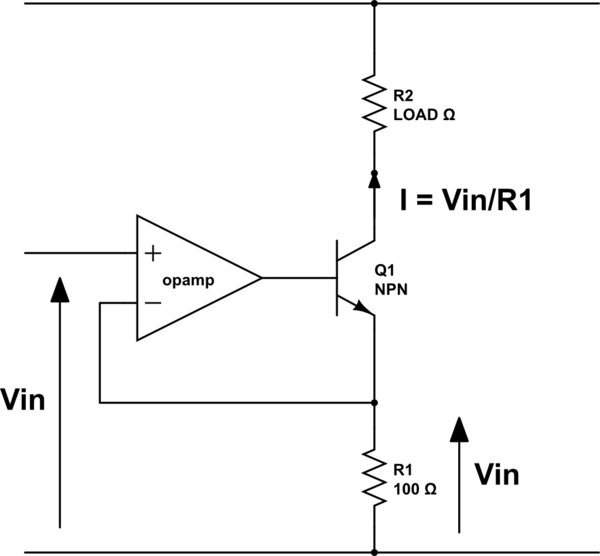
I've successfully used Vcc tied loads like this in constant current circuits: -

schematic

simulate this circuit – Schematic created using CircuitLab

The op-amp has negative feedback from the emitter and therefore the emitter voltage must be at the same potential as the input. This means the current through the BJT = \$\dfrac{V_{IN}}{R1}\$

You can also use a PNP BJT and an op-amp mirrored up to the positive supply rail for ground coupled loads.

\$\endgroup\$
2
  • \$\begingroup\$ This is basically what Dave Tweed already suggested in the comments above. I think this is the best solution to my problem, since (as far as I understand) this configuration will make the feedback gain at the op amp almost independend of the load (until we try to sink more current than the load permits) \$\endgroup\$
    – Medo42
    Commented Apr 28, 2014 at 10:19
  • \$\begingroup\$ On second thought (and after playing around in the simulator some more), this creates a new problem: Once I try to set a current that can't be achieved, the op amp will turn the transistor fully on and then continue to rise to the positive rail. The feedback gain becomes essentially zero, so it can take a long time to recover and reach the linear region again. Do you know how I could force the op amp to stay within the linear region? \$\endgroup\$
    – Medo42
    Commented Apr 30, 2014 at 14:46
1
\$\begingroup\$

You could try clamping the feedback voltage (eg. with a diode).

But first I would try to speed up the circuit- get rid of R1, which inserts a pole for no good reason that I can see, and try to reduce C1 to something like 100pF.

\$\endgroup\$
1
  • \$\begingroup\$ Removing R1 dramatically reduces ringing, thanks! In the actual circuit it is currently needed since something else also connects to the Q1 base, but I can try to change that or at least reduce its value. \$\endgroup\$
    – Medo42
    Commented Apr 25, 2014 at 14:02
1
\$\begingroup\$

I'm going to assume you are using the first schematic.

Since you only need a maximum of 50 mA output current, the TIP102, which is a 3 Amp Power Darlington, is totally inappropriate! The large junction capacitance causes signal delay and severely limits closed-loop bandwidth. This is also causing most of the circuit instability.

The op-amp has a 20 mA output current capacity, and so the required additional current gain is just over x2.5 to reach the 50 mA maximum setpoint, so any moderate gain 50V junction transistor will do, however, a MOSFET will perform better.

As already mentioned by others, having the load on the emitter is a large part of the problem. The TIP102 Darlington transistor has an internal 10 KΩ resistor protecting the base. With the external 10 KΩ resistor in series with this internal resistor, loop compliance and signal delay is made even worse. (The TIP102 is typically used as a low-parts-count switching transistor, not as a linear signal transistor.)

Since the LT1013 OpAmp is already internally compensated to be stable at unity gain, the external 1nF (0.001 μF) capacitor is actually causing problems. It is unnecessary once the TIP102 is replaced. It should be possible to eliminate any remaining instability by refining layout.

The minimum load resistance of 10 Ω can easily have a maximum current of 50 mA imposed, dropping only 0.5 Volt.

Lower current settings will have increasing inaccuracy due to input offset voltage. Since you are operating down to very low signal levels with this design, offset compensation is vital! (The maximum load resistance of 10 KΩ will draw only ~ 3.6 mA from the 36 Volt supply, requiring an input signal of, at most, 12 mV!)

The input offset voltage can be minimized by using matched 1% input resistors. In this design, the non-inverting input needs a precisely matching 10 KΩ, however, you may safely omit both input resistors or use small values (like 470 Ω 1%).

Others have already suggested that you place the load on the collecter, and I agree. This will improve compliance, bandwidth, and circuit stability. If you want the greatest compliance, use a MOSFET.

At the maximum setpoint current of 50 mA, with a current sense resistor of 33 Ω, the input and feedback voltages are 1.65 Volts.

With a supply voltage of 36 VDC, the maximum current load voltage is ~ 33 Volts. Therefore, the maximum permissable load resistance at 50 mA is ~ 660 Ω. For higher resistances, the input control signal must be reduced to maintain loop compliance.

The maximum resistance of 10 KΩ will draw only ~ 3.6 mA, requiring a control signal of, at most, 119 mV. In order to impose 50 mA on 10 KΩ, the supply voltage would have to exceed 500 Volts (and dissipate 25 Watts in the load).

\$\endgroup\$
1
  • \$\begingroup\$ I actually ended up using a voltage follower configuration as shown in my question for the circuit, but using an FQP13N06L MOSFET instead of the TIP102, and yes, I didn't need the compensation capacitor. \$\endgroup\$
    – Medo42
    Commented Dec 17, 2014 at 10:36

Your Answer

By clicking “Post Your Answer”, you agree to our terms of service and acknowledge you have read our privacy policy.

Not the answer you're looking for? Browse other questions tagged or ask your own question.