5
\$\begingroup\$

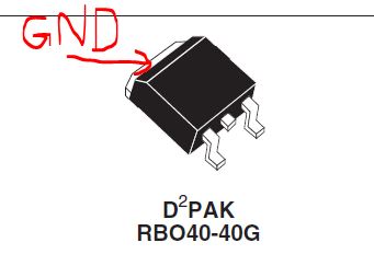
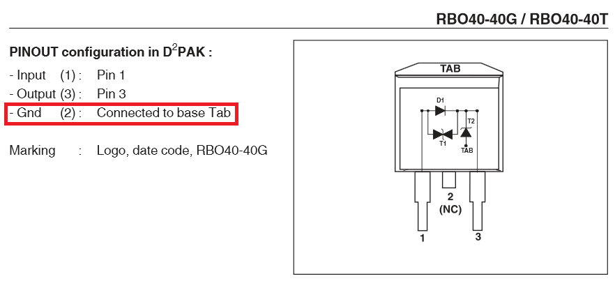
I'm looking to use a RBO40 reverse battery & over voltage protection. I was unable to find the RBO40-40T (with 3 pins) anywhere so had to get RBO40-40G, which is slightly different, it has the middle GND pin cut and the data sheet says this goes to the TAB instead.

I'm not really up on this chip packaging, how am I meant to connect this GND when the TAB is a flat metal surface on the back of the chip?

Data sheet is here

Thanks

\$\endgroup\$

2 Answers 2

7
\$\begingroup\$

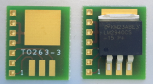
The middle pin that is cut and the TAB are both shorted to GND. When you are placing the part on PCB create a PCB footprint for the flat surface and connect the pad to ground. This is also used to dissipate heat. The part you have is a SMT part.

enter image description here

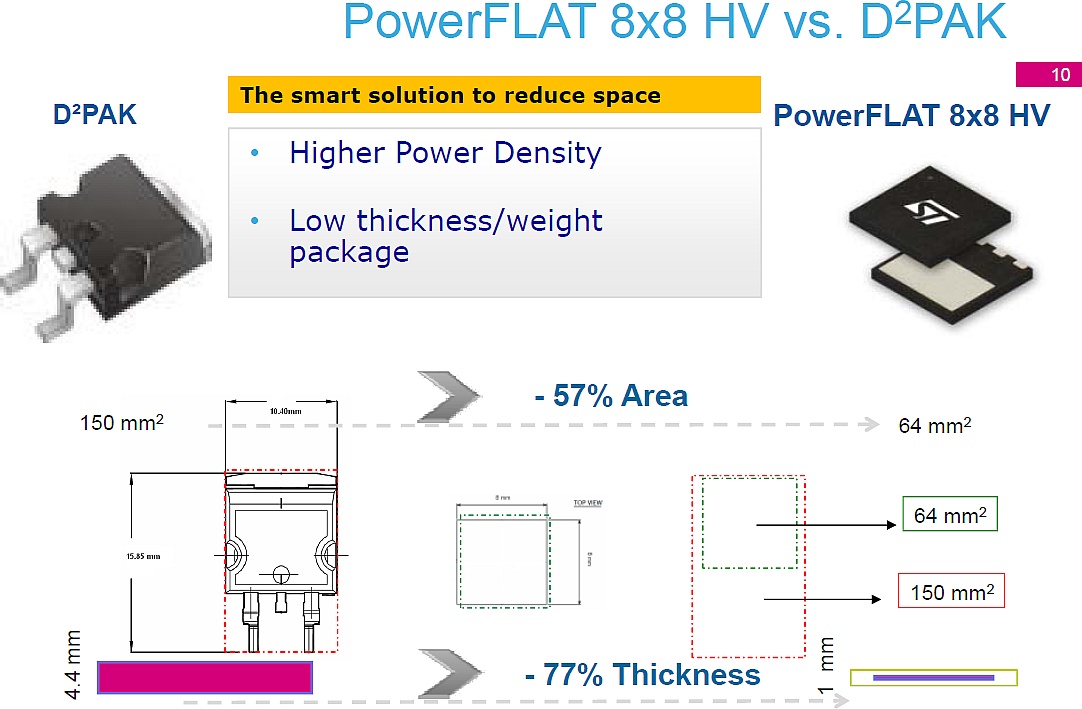
If you are soldering wires, solder the GND wire to the flat TAB. You will find \$D^2PAK\$ package in the attach image below. Like the TO-220 package \$D^2PAK\$ is mostly used in power products.

enter image description here

If you look at page 5 and page 9 of the datasheet you will see more infomation about the package.

References:

\$\endgroup\$
1
  • \$\begingroup\$ Great, was just confirming this really. I will solder to the tab. Not ideal but ok for a prototype right \$\endgroup\$ Commented Jul 7, 2015 at 11:51
4
\$\begingroup\$

Here is an image about the required layout/footprint. It is clearly shows how you should design and solder your component.

enter image description here

By the way the datasheet holds the answer for your question, always read it in detail. I took this picture from it. enter image description here

\$\endgroup\$
1
  • \$\begingroup\$ Yes, I read that, I just thought that was odd and wanted to check. \$\endgroup\$ Commented Jul 7, 2015 at 12:00

Your Answer

By clicking “Post Your Answer”, you agree to our terms of service and acknowledge you have read our privacy policy.

Not the answer you're looking for? Browse other questions tagged or ask your own question.