0
\$\begingroup\$

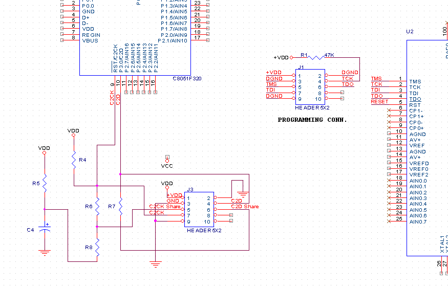
I'm working on a Silicon labs MCUs. Few of it's MCU requires JTAG while few requires C2 interface for flash programming and debugging. Below I've uploaded a image for JTAG & C2 Interface. And it's been the same adapter used for both the interface.obviously they are compatible. JTAG interface I understood clearly but for C2 interface I have doubts regarding their pins connections.

C2 & JTAG interface

I went through adapter's user's guide(page no 2) for better understanding, where it states 2 pins as C2CK & C2D pin share. I didn't understood what you mean by this and how this resistive network are used for C2CK & C2D pin sharing? Because no such circuit diagram(resistive network for C2 interface) is given in user's guide. And when I studied about C2 interface from other sources, it was mentioned only about C2D & C2CK & nothing about such pin sharing.

Another thing, TCLK(CLOCK) & TDO(Data out) of JATG is share by C2D and TMS(mode state) & TDI(Data in) are shared by C2CK. can someone actually explain what is actually happening here?

So my question's are-

  1. How would we understand C2CK & C2D pin sharing means such resistive network?

  2. How C2 & JTAG interface are made compatible with this design? (P.S. I'm not sure about this question as I did not understand it completely or I can just assume both the Interface are compatible with this design)

\$\endgroup\$
1
  • 1
    \$\begingroup\$ C2 and JTAG are NOT compatible. SL simply built an adapter that can accommodate both protocols (using the same 10-pin cable). C2 is for programming and debugging only, and is used on smaller chips (it uses only 1 extra pin). JTAG can do much more, and is used on larger chips, where its boundary-scan features are useful. \$\endgroup\$
    – Mark
    Commented Jun 17, 2016 at 6:31

1 Answer 1

1
\$\begingroup\$

Here's an application note that covers Pin Sharing Techniques for C2.

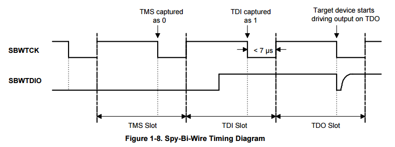
Basically, it looks like another 2-wire serial interface like TI's Spy-By-Wire. It's probably time-division multiplexing like SBW does, where an internal FSM knows when to sample to de-mux to TCK, TMS, TDI and TDO. Instead of those four wires required, it'll basically clock out TDI, TMS, and then it will sample TDO from the DUT on the data line. Some implementations I've seen also throw the actual debug clock on the data line. Here's what TI does:

enter image description here

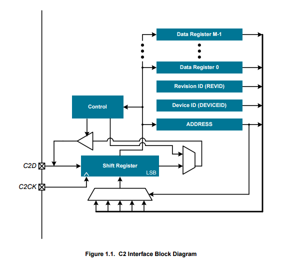
It looks like C2 isn't strictly JTAG on that bus, but rather they have some set of instructions that are supported there, seen in this app note. Very similar to JTAG, but not 100% the same.

enter image description here

For your case, it looks like you actually don't have to worry about pin-sharing. It looks like that is intended for applications on very low pin-count devices, or if you have very high pin utilization and those I/Os are used in the actual application. In your case, those pins are being used only for programming, so I think you can ignore the pin-sharing concerns.

To me, seems like you only need pin 4 and pin 7 from the header to your MCU. I think it's good practice to put some 0R resistors in series with those signals in case you want to tune those values, in addition to putting a small 0.1uF decoupling cap near the connector. You could also consider ESD protection on those lines, keeping capacitance in mind.

So, for #1 -- you don't need to worry about it unless you are going to use those I/O pins for something else besides programming. The resistors help in "isolating" the loads so the programmer can maintain sufficient signal integrity for programming your part.

For #2, it's a two-wire multiplexed bus as I described above that is very similar to JTAG on the inside of the part, they have simply streamlined and serialized to cut down on pin count.

\$\endgroup\$

Your Answer

By clicking “Post Your Answer”, you agree to our terms of service and acknowledge you have read our privacy policy.

Not the answer you're looking for? Browse other questions tagged or ask your own question.