1
\$\begingroup\$

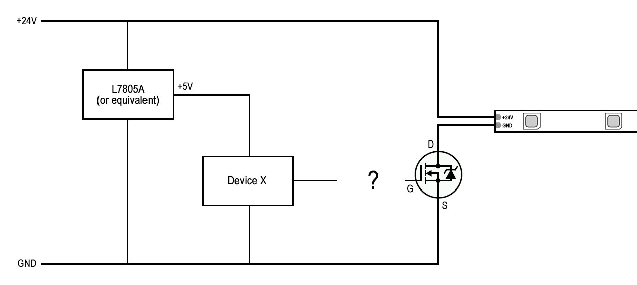
I'm trying to control a 24 V LED strip with a device that has its own control mechanism and PWM output. (The output PWM frequency is 1 kHz.) The device itself requires 5 V, and since it does not draw that much power so I'm planning to use a standard voltage regulator there, not that interesting.

My problem here is that the device's PWM output logic is rather weird. It's logic LOW is 2,5 V while a logic HIGH is 5 V.

Here is my schematic:

Schematic

As for the N-channel mosfet, I'm planning to use the IRLB8721 (datasheet). But this one won't turn off on a 2,5 V logic LOW by my device. The question is; how can I "shift" this logic LOW down to GND?

Almost all Google searches I've tried lead me to logic level shifters that most often let 3,3 V logic devices connect with 5 V logic devices and vice versa...

I did find two interesting topics here on the Electrical Engineering Stack Exchange with almost the same problem, but I could not figure out how to translate the solutions posted there to my specific problem:

Translating to “below ground” logic levels

-5/0 volt to 0/5 volt logic levels?

\$\endgroup\$
6
  • 1
    \$\begingroup\$ Take BJT with three diodes on the base. That will make minimum voltage two open it somewhere around 2.4V to 2.8V \$\endgroup\$
    – user76844
    Commented Jan 23, 2017 at 21:48
  • \$\begingroup\$ Do you mean to take a BJT instead of the N-channel mosfet I'm planning to use? Or to add the BJT in front of the mosfet? Could you please elaborate? \$\endgroup\$
    – empewoow
    Commented Jan 23, 2017 at 22:03
  • \$\begingroup\$ Instead the MOSFET \$\endgroup\$
    – user76844
    Commented Jan 23, 2017 at 22:04
  • \$\begingroup\$ OK, but I'm planning to use the mosfet there because of the high power demand for the LED strips. I forgot to mention that in my story. Is there a way to do this with the mosfet? \$\endgroup\$
    – empewoow
    Commented Jan 23, 2017 at 22:12
  • 1
    \$\begingroup\$ Many ways. You could use OpAmp and rescale voltage any way you want \$\endgroup\$
    – user76844
    Commented Jan 23, 2017 at 22:14

5 Answers 5

2
\$\begingroup\$

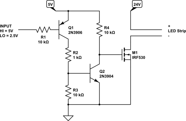
How about some simple bipolar inverters like below?

schematic

simulate this circuit – Schematic created using CircuitLab

With 5V at input, Q1 is turned off so R4 pulls the gate high, turning on M1 and your LED strip. With 2.5V at the input, Q1 is turned on which turns on Q2, which pulls the M1 gate low which shuts off M1 and your LED strip goes off.

You'll need to refine the circuit, check the resistor values, find a better M1, make sure response is fast enough for your PWM frequency.

\$\endgroup\$
1
\$\begingroup\$

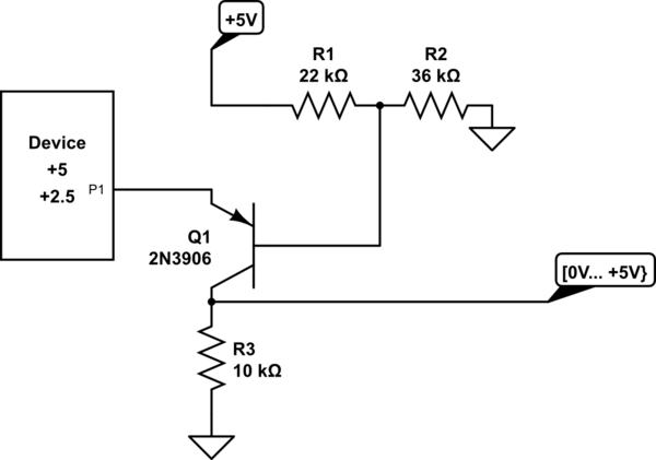
If you want a noninverting translator, one transistor will do it.

schematic

simulate this circuit – Schematic created using CircuitLab

This is a so-called 'grounded base' configuration, it gives the voltage amplification you require, but no current gain (the 'Device' will have to source 0.5 mA in order to put 5V across the R3 load resistor). The R1, R2 values set the base at 3.1V quiescent (it should switch at about 3.7V from 'Device').

This circuit does not try to be a fast switch, but a simple one. R3 and the 'Device' output current determine how fast the gate capacitance is charged and discharged.

\$\endgroup\$
1
  • \$\begingroup\$ As this solution was the easiest and required the least parts, I simulated this one and tried it out in a prototype. Turns out it works flawlessly for my application. When checking the signal on a scope the performance turns out not perfect (both edges have some lag and are less sharp-edged than original signal) but in practice there is no negative effect on the experience of the LED strip light. Many thanks for this simple circuit. \$\endgroup\$
    – empewoow
    Commented Jan 25, 2017 at 15:00
0
\$\begingroup\$

That is probably not an output with a logic digital signal, or else it might be the first device in the world that outputs such a signal. Could the output be a darlington output, which is capable to drive the leds ?

What happens to the PWM signal when you connect a resistor to 5V or to GND ? Do the test for example with a 1k resistor. When you know the impedance for a high and low, then you can decide how to translate that signal. Perhaps a optocoupler can be used to translate the signal or perhaps a transistor with a few diodes as suggested.

\$\endgroup\$
1
  • \$\begingroup\$ Yes that is possible. I'm not sure what this pin I'm probing is used for internally. But the output is almost usable, except for the 2,5 V minimum voltage... I will try the resistor thing tomorrow and let you know. Thanks. What is it I'm hoping to find when I add the resistor by the way? What can I expect on the signal? \$\endgroup\$
    – empewoow
    Commented Jan 23, 2017 at 22:15
0
\$\begingroup\$

At first check; Is it really +5V =high +2,5V=low.

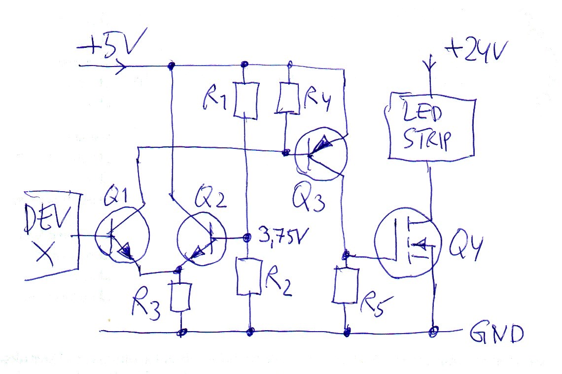
Assuming yes: Use a comparator that outputs 0V or +5V directly to the gate of the mosfet. Comparator tests, if device X outputs more than 3,75 V. If yes, then give +5V to mosfet's gate.

A proper comparator that operates from single +5V supply, can produce 0V and +5V output levels and can sense properly +5V is tricky. Here it is as a discrete part implementation

enter image description here

Parts must calculated starting from the end

  • R5 must pull the gate down fast enough
  • Q3 must push enough collector current to lift the gate near +5V
  • Q3's base current = the collector current/hfe
  • for reasonable turn off speed, R4 must take at 0,7 V at least as much as Q3 needs base current; that is R4 < or = (0,7V/ Q3's base current)
  • Ri and R2 produce the treshold 3,75 V to Q2
  • R3 gets about +3,05 V. R3 = 3,05 V/(Q3's base current + 0,7 V/R4)
  • the 3,75 V reference should not teeter. Let (R1 parallel R2) to be five times R3 or less. Add a capacitor parallel with R2, if needed.
  • solve R1 and R2 from the wanted voltage and max parallelled resistance.

At first take Q1 = Q2 = 2N1711, Q3 = 2N2905. 2N3704 and 2N3904 should be ok, too.

Simulate before building a prototype

\$\endgroup\$
3
  • \$\begingroup\$ Thanks for this elaborate solution. What would be the advantage of this circuit over the simple "grounded base" configuration? (See one of other answers.) And yes, the pin I probed is really 2,5 to 5 V and has the biggest amplitude, compared to other pins I probed. All started at 2,5 V or more. \$\endgroup\$
    – empewoow
    Commented Jan 25, 2017 at 15:05
  • \$\begingroup\$ @empewoow Check at first, if something pulls your signal up; it is: Already a too low Ohm resistor or other part is connected between your output and the +5V. Answer: This solution can be faster because as much current as needed for fast mosfet switching can be pushed and pulled to/from the gate. The simple version is limited to how much your device X can push out. But if its speed is enough, use the simple version. NOTE: The simple version does the same for the mosfet than Q1 in my version does for Q3. In both cases the controlling voltage is compared to the reference by a comparator circuit. \$\endgroup\$
    – user136077
    Commented Jan 25, 2017 at 15:34
  • \$\begingroup\$ @empewoow (continued) Check also, if the output in dev X needs a pulldown resistor that still is not connected. About he speed: if you blink the leds at few hundred Hz, the simple solution might be fully usable. Simulate it first and see how long the transitions take when compared to the switching period.Those transition times should be max. a few percent ot the period. \$\endgroup\$
    – user136077
    Commented Jan 25, 2017 at 15:52
0
\$\begingroup\$

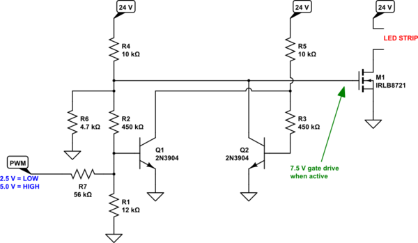
Well, you have a whole lot of possible answers. I'm going to assume you still want to use your MOSFET device, the IRLB8721. A \$V_{GS}\gt 6\:\textrm{V}\$ looks like it operates very solidly then. The total gate charge is about \$12\:\textrm{nC}\$ and I've set up a circuit that should deliver that charge in under \$20\:\mu\textrm{s}\$, which may be fast enough given the PWM rate.

schematic

simulate this circuit – Schematic created using CircuitLab

The gate voltage should switch between \$0\:\textrm{V}\$ or \$7.5\:\textrm{V}\$ when the input PWM switches between \$2.5\:\textrm{V}\$ and \$5.0\:\textrm{V}\$. The circuit includes hysteresis, will keep the drive voltage to the gate of the MOSFET safely low enough, is widely tolerant of BJT \$\beta\$ (anything from 100 to 300 is fine), accepts reasonable variations in the saturation current of the BJTs, and provides about \$500\:\textrm{mV}\$ width for the hysteresis band, which should provide reasonable noise immunity as well.

It doesn't use boutique parts and should be relatively cheap. Figure about an additional \$4\:\textrm{mA}\$ load on your \$24\:\textrm{V}\$ supply rail. (It doesn't need or use anything from the \$5\:\textrm{V}\$ supply rail.) It's also easy to tweak the gate drive for other MOSFETs which may require higher \$V_{GS}\$, especially given access to a \$24\:\textrm{V}\$ rail (as you currently have.)

\$\endgroup\$
2
  • \$\begingroup\$ I also simulated this option and it works as expected. Thanks. If the "grounded base" configuration gives me any problems I'll try this or the other options. Using the 5 V rail is no problem for me. \$\endgroup\$
    – empewoow
    Commented Jan 25, 2017 at 15:03
  • \$\begingroup\$ @empewoow Using the 5 V rail would limit your mosfet choices. Using the 24 V rail means every mosfet is workable. \$\endgroup\$
    – jonk
    Commented Jan 26, 2017 at 6:58

Your Answer

By clicking “Post Your Answer”, you agree to our terms of service and acknowledge you have read our privacy policy.

Not the answer you're looking for? Browse other questions tagged or ask your own question.