11
\$\begingroup\$

I am currently working on my first microcontroller hardware design; I had a microcontroller class in college, but it focused on the software side of things, and used a pre-made development board (for the Freescale 68HC12).

I have a question that I hesitate to ask because it seems fairly basic, and perhaps even obvious, but at the same time I have not been able to find a clear answer while searching through either datasheets or online forums.

I have decided on an STM32F7-series chip, and I am running into this query while planning out its basic power and ground connections. I see a total of 12 Vdd pins on the 144-LQFP package (9xVdd + 1xVdda + 1xVddusb + 1xVddsdmmc), but only 10 Vss pins. Quick aside: I briefly considered Microchip's dsPIC33F for this project, and I noticed a similar imbalance (7 Vdd pins and 6 Vss pins).

I have been reading some introductory hardware design documentation, and the importance of decoupling caps placed close to the device for each Vdd/Vss pair is always emphasized forcefully for high-speed designs. I wonder what I should do for those Vdd pins which have no obvious Vss pairing. My PCB will certainly be incorporating a ground plane layer, so I could simply decouple those un-paired Vdd pins directly to the plane, but I just always got the sense that those Vdd/Vss pin pairings were important.

Am I missing something obvious?

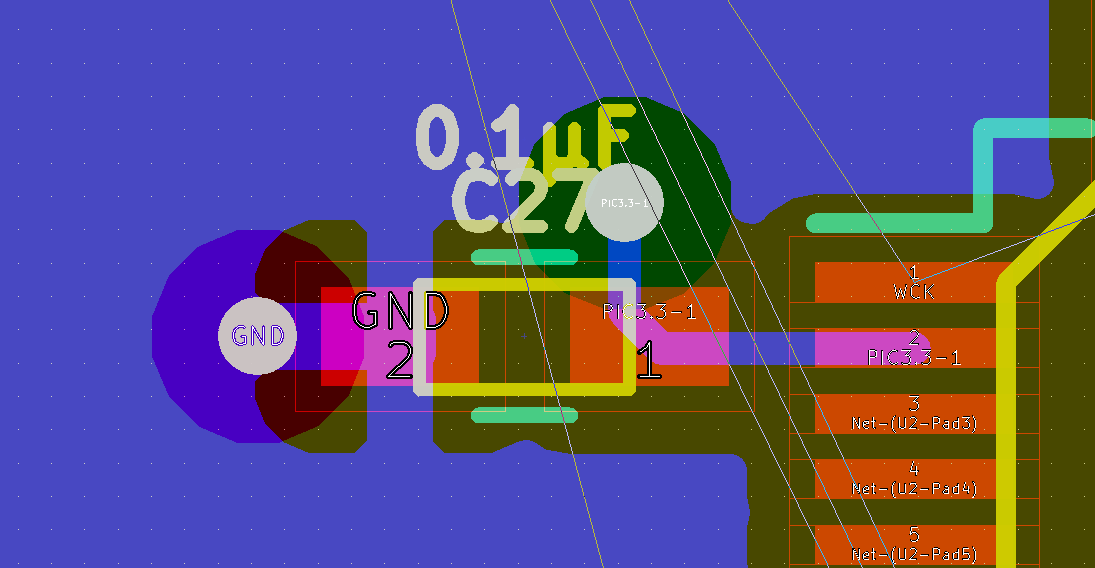
I have included a couple of pictures below, which show my current strategy for decoupling both a Vdd/Vss pair and a single Vdd pin. Please do let me know if there is an obvious issue with either method.

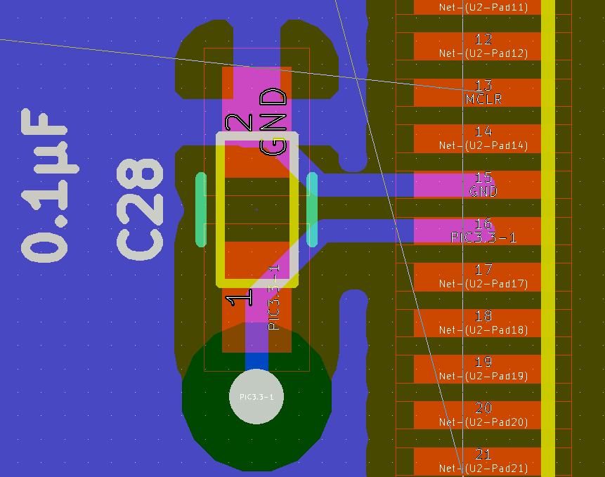
Decoupling a pair

Decoupling a single Vss

\$\endgroup\$

3 Answers 3

23
\$\begingroup\$

As a chip maker, it's easy for me to explain the cause of the imbalance. It's that there are several different rings of VDD in the IC for different purposes, but only a single ground. The different VDD rings can be in different voltages, but the ground is always at zero volts.

So for the ground, there is a solid copper rectangle in the leadframe (that's what the IC pins extend from) under the die for the ground. Internally, there can be dozens of pads that are all down-bonded to the ground copper. This way the ground can be quite solid across different parts of the IC, which minimizes substrate currents - current flowing through the copper will not cause problems such as latch-up in the IC, unlike strong substrate currents that cause latch-up conditions.

So, internal to the plastic casing in the IC, there are, more or less, the GND/VCC pairs that you mention in your question. But as for the ground, due to the ground pad in the leadframe, not every GND pin needs to extend out from the IC package - the ground copper inside the IC package is strong enough.

\$\endgroup\$
0
8
\$\begingroup\$

Just connect the remaining VDD pins to the ground plane via decoupling capacitors. It is not always necessary that power and ground pins be equal. If you have a solid ground reference throughout the circuit, it will work fine.

\$\endgroup\$
1
  • \$\begingroup\$ Thanks; I suspected as much, but I just couldn't find a clear answer anywhere I looked. \$\endgroup\$
    – Don Joe
    Commented Oct 1, 2017 at 6:58
0
\$\begingroup\$

Besides the other reasons... the stm32f7xx is the successor of the successor... of a chip where there where more ground pins than what you see now on your F7. The F4 and the followup F7 have vcore decoupling on two pins that where GND on stm32F1xx and 'F2xx ......

\$\endgroup\$

Your Answer

By clicking “Post Your Answer”, you agree to our terms of service and acknowledge you have read our privacy policy.

Not the answer you're looking for? Browse other questions tagged or ask your own question.