0
\$\begingroup\$

Problem:

My issue is that the momentary switch with NAND latching logic that I have designed is not functioning consistently. It does work as intended at first, but then fails to work after repeated testing, never regaining functionality.

Question:

Is there something wrong with the way I have designed my logic that is determining the voltages at the gates of the two different FET's (DISP FET and MAIN FET) in my circuit? Specifically, my choice of R4, R5, and D4? Or is it something else entirely?

Background Info:

  • The circuit that I am making is a back-up power bank of lithium ion batteries, and when the momentary switch is pressed ("SW" in the schematic", this provides power from this back-up power bank to the main power bank (through the "BOARD-" terminal shown in the schematic).
  • The "SN74" chip is a latching double NAND, part #: SN74LVC2G00DCTR.
  • The CHRG IND terminal is NC to ground.
  • The diode "D4" is rated 10V, 100mA, part #: 1SS367,H3F
  • I designed the latching logic of my circuit based on Fig. 5 from the example on this site.
  • The purpose of the DISP FET is to allow the battery capacity display to turn only when there is a charger plugged in, but not turn the rest of the circuit on (the USB ports, switch on the LED, and the power supply from the batteries to "BOARD-")

Testing of the Issue:

I have the lithium ion batteries at 41V, and then my buck converter is outputting a consistent 5V everywhere it is tied to, which I verified with a multimeter. I also did a continuity test across the board, there are no shorts between any of the power rails or ground, or across any of the components.

My tests

  1. When I first assembled the PCB, it was working exactly as intended. So, I push the main momentary switch of the circuit that provides the functionality and as a result, The USB ports, the LED on the switch itself, the battery capacity display, and the output to "BOARD-" are all on. Then, I leave my circuit for 10 minutes. I come back, push the switch again, and the switch does not turn on. The way that I verified this is that I tested the voltage at the output of the SN74, and it stays at ground, it does not go to 5V as it did when it worked in the first place.
  2. After this initial failing, I put a scope meter on the gate signal, and sometimes I would see the gate voltage spike to about 560mV, so not enough to turn on. Other times, it would spike all the way to 5V, but not hold the high state, but just go back down to ground. Other times, the switch would turn on without me even pressing it, upon me providing power to the board.
  3. I swapped the NAND IC for a fresh one, and the circuit would work. But, it would then soon fail again as before. I tried removing the diode "D4", creating an open circuit there, and then the button would work as intended. However, it would then also soon fail afterwards.
  4. I also tried shorting across the diode, and it seemed that when it was working, the button would turn on, but not turn off. Then, just as before, it would also just not even turn on anymore.
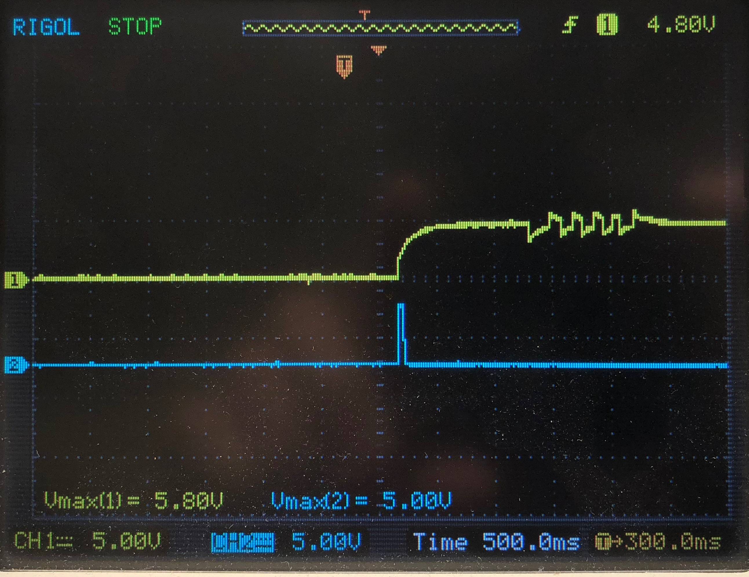
  5. I tried putting a scope meter on the input of A1, see oscilloscope below for output. The blue line is the voltage at the output, so pin 1Y , going to the gates of the FETs, and the yellow line is the voltage at the input pin 1A. The max voltage of 5.8V at the input pin 1A did not exceed the 6.5V maximum rating of the SN74. The ramp up and ramp down of the yellow line is from me pushing the momentary switch.
  6. I took the SN74 off, and connected the CD4011B to the circuit using a breadboard and wires. Still, the circuit did not function.

enter image description here

Conclusion:

All these testing results are proving to be inconsistent and I can't seem to figure out what the cause of the issue is. Ultimately, I know that my design did work for 10 minutes, and then the failures started, so that would perhaps be the biggest clue.

\$\endgroup\$
13
  • 2
    \$\begingroup\$ i do not think that anyone will spend the time to decipher the "wall of text" that you posted .... please edit your question to make it more readable ........... also, the schematic is incomplete \$\endgroup\$
    – jsotola
    Commented Jun 20, 2018 at 18:01
  • \$\begingroup\$ Good call, I modified it, hopefully this is better for people. I included a lot of info because I think it is all relevant to the issue. \$\endgroup\$ Commented Jun 21, 2018 at 1:10
  • \$\begingroup\$ Why don't the ICs all share a common ground? U2 and U3 grounds are connected to.. what? \$\endgroup\$
    – bmow
    Commented Jun 21, 2018 at 1:41
  • \$\begingroup\$ "I put a scope meter on the gate signal, and sometimes I would see the gate voltage spike to about 560mV, so not enough to turn on. Other times, it would spike all the way to 5V" Show oscillograms! \$\endgroup\$
    – winny
    Commented Jun 21, 2018 at 7:46
  • \$\begingroup\$ I have nothing useful to say. Just wanted to mention that when I am looking at something like that I am missing the 80s... when engineers were priding themselves on doing same things we do now with 10 times less components. \$\endgroup\$
    – Maple
    Commented Jun 21, 2018 at 7:50

2 Answers 2

1
\$\begingroup\$

Your latching circuit design will briefly apply up to 10V to U1 pin 1, when the switch is released, due to the action of C1. Since the chip's absolute maximum input voltage is 6.5V, this will damage or destroy the chip, as evidenced by the burning and smoking you observed.

The example latching circuit you referenced calls for a CMOS logic gate such as CD4011, which has a 3V to 18V supply range, and can tolerate a 10V pulse. But your circuit uses a 74LVC00, which can't.

\$\endgroup\$
7
  • \$\begingroup\$ I monitored the voltage on that 5V line everywhere, I did not see it spike or stay sustained above 5V. Also, its not consistently burning, that is the thing, sometimes it does and sometimes it does not. Sometimes it will just start working out of nowhere, and then again it will just stop working all together. \$\endgroup\$ Commented Jun 21, 2018 at 1:11
  • \$\begingroup\$ It's not necessarily the 5V supply line - it could be any of the IO pins. \$\endgroup\$
    – bmow
    Commented Jun 21, 2018 at 1:36
  • \$\begingroup\$ Could also be a brief over-voltage or under-voltage that doesn't show up on the multimeter, but is still enough to cook the chip. \$\endgroup\$
    – bmow
    Commented Jun 21, 2018 at 17:08
  • \$\begingroup\$ Edited my answer with a predicted cause of the over-voltage, based on analysis of your latching circuit. \$\endgroup\$
    – bmow
    Commented Jun 21, 2018 at 18:19
  • \$\begingroup\$ I edited my post, adding the oscilloscope plots from the voltage on U1 pin 1. The voltage did not exceed 6.5V. I also tested this on VCC, and it did not exceed 6.5V there as well. I also swapped the SN74 with a CD4011 as you were indicating, and the circuit did not function. The PCB is pretty damaged at the SN74 location now from all the testing, so I will try and assemble another one, to see if that is the cause of the issue. \$\endgroup\$ Commented Jun 21, 2018 at 22:03
0
\$\begingroup\$

The problem was with the way that I had constructed my "glue logic" around the two MOSFETs. I made a number of changes:

  1. Replaced the "D4" diode with an OR gate, with inputs from the charge indication and the output of the SN74, and the output going to the DISP FET.
  2. Tied the high side of the LED switch to the output of the SN74, with a 220 Ohm resistor from the low side to ground. This allowed toggling the LED of the momentary switch itself with the momentary switch. This was the change that actually fixed the root of the problem, all the other changes below were optimizations.
  3. Tied the enable pins of the TPS2511s to the output of the SN74, as bmow was suggesting. So, removing the 100kOhm tie to 5V as I had it before, now the enable is toggled by the momentary switch. The problem here was because the low-side of the LED and the TPS2511's was floating when the MAIN FETs were not conducting. Although not a necessary change, I think it improved the design because I removed two diodes, and the momentary LED was no longer turning on when the MAIN FETs were off. It was doing this because there was a path from the LED to the grounds of the TPS2511's.
  4. Changed the RC combo on the input of the SN74 to 1MOhm and 1uF, instead of 10MOhm, as this was a very high resistance, and so it would act more as an open circuit, which could cause unreliability in the switch operation.

With these changes, the circuit worked as intended, many times, reliably. I did not observe any 10V spikes on the input of the SN74, the highest I saw was 5.8V. However, I will add the zener diode on the VCC input as Bruce Abbott was suggesting, because I did not do these tests with the load connected, and I can see inductive loads being a problem.

Thank you everybody for your help!

\$\endgroup\$

Your Answer

By clicking “Post Your Answer”, you agree to our terms of service and acknowledge you have read our privacy policy.

Not the answer you're looking for? Browse other questions tagged or ask your own question.