1
\$\begingroup\$

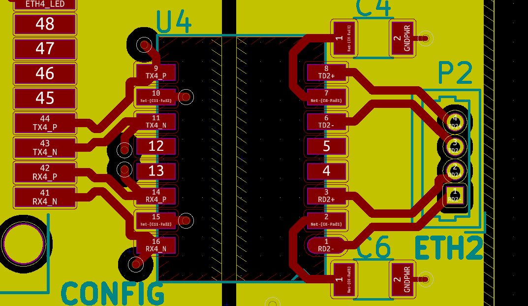
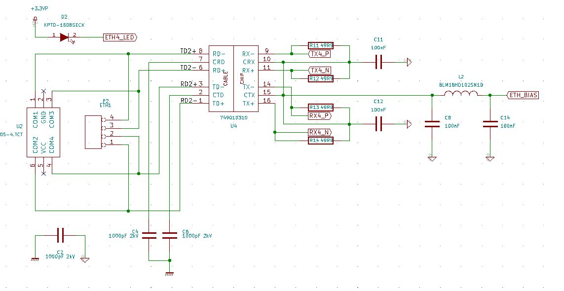
I'm designing a board (with KiCAD 5.1.0) besides other I need to properly route two ethernet ports and the whole board should be kept as small as possible (50x82mm). The guidelines of components (magnetics) give some hint about trace layout but the main component (where the two ports originate) is not very well documented... anyway I looked around and did my best. The final result lead me to some question:

enter image description here

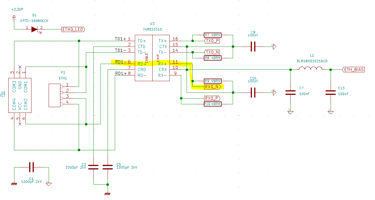
On this port I had to reverse the magnetics ports to avoid vias and complex traces to connect the main component with magnetic IC itself:

enter image description here

Please note that the ethernet connector is not an RJ45 since I have very big space constraints and RJ45 should not fit in the assembly.

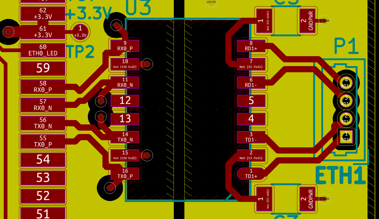
In the first port I needed to reverse the polarity of the magnetic input for the same reasons as above:

enter image description here

enter image description here

The effect of these workarounds are negligible on the overall performance? Take into account that both ethernet ports will be connected to a very near device (around 20cm of cable length or less) and that the overall troughput on such ports will never exceed 10Mbits.

Differential pairs have been setup to have 100ohm impedance (the board will have a standard 4 layer FR4 stackup).

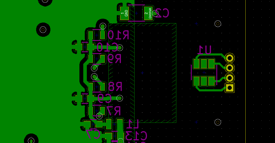
To keep everything small and avoid complex traces I placed some of the passive components on the top layer and some other on the bottom side:

enter image description here

Of course I needed to place some vias on the forbidden zone below the magnetic IC... is it soooo wrong?

Magnetics IC = Wurth 749010310.

Any comment will be appreciated. Of course I can share the whole design if someome wish/need to investigate further.

\$\endgroup\$

2 Answers 2

1
\$\begingroup\$

Passive placements: Place them on the same side of the transformer. A couple of 0402 will not increase your board size. You should avoid vias on the Ethernet signals.

Vias near the transformer: You should avoid these, if you have to pass the isolation tests.

If board space is an issue, you can use a connector with integrated magnetics.

\$\endgroup\$
1
  • \$\begingroup\$ The board is been successully printed, tested and it's working fine even with my infringements. In the next release I will try to fix them... I have big costraints on all 3 axes and none of RJ45 connectors I know (with or without magnetics) should fit. \$\endgroup\$
    – weirdgyn
    Commented Jul 30, 2019 at 13:20
-1
\$\begingroup\$

If you have control over both ends. Then you can omit the Ethernet transformer in one or both ends to make it smaller. Just replace the transformer with 4*10nF capacitors... You still need to restore the DC-offset that your Ethernet PHY require. But it will for sure become much smaler. The only "bad" effect is that you lose the 1500 Volt galvanic insulation.

\$\endgroup\$
1
  • \$\begingroup\$ Almost true, but not all PHYs support capacitive coupling, and it is generally only used on fixed 100Mbps links and definitely not recommended, if even possible at all 10Mbps links. I think this answer does not address the question asked about PCB routing. \$\endgroup\$
    – Justme
    Commented May 9, 2023 at 16:10

Your Answer

By clicking “Post Your Answer”, you agree to our terms of service and acknowledge you have read our privacy policy.

Not the answer you're looking for? Browse other questions tagged or ask your own question.