[![the output of my GPIO is 1.8V which is pulled up to 3.3V using a 4.7K resistance and that gpio is connected to the gate terminal of a P-channel mosfet, when i measure voltage across the gate terminal it results in 1.8V and i got 1.8325V by nodal analysis at gate terminal but i'm not getting why so, can anyone provide me what things should i learn to solve these kind of problems][1]][1]
-
1\$\begingroup\$ Please add a schematic of your circuit, and datasheets of both the MCU and the transistor. \$\endgroup\$– SorenpCommented Oct 18, 2019 at 12:38
-
\$\begingroup\$ Welcome to the site. Please realise this is not a free design house, homework-answering service or an on-line technical encyclopedia, copied out to you on demand. People will help you take the next step if your question shows you've done as much as you possibly could on your own - which yours doesn't, I'm afraid. Please edit your question and greatly improve it. Show your work and findings so far in considerable detail with a schematic. The schematic tool here is easy to use. The better the quality of question, the better the quality of the answers you will attract. Again, a warm welcome. \$\endgroup\$– TonyMCommented Oct 18, 2019 at 12:39
-
2\$\begingroup\$ Probably your ESD protection diodes towards the 1v8 GPIO supply rail start conducting. \$\endgroup\$– OldfartCommented Oct 18, 2019 at 13:12
-
\$\begingroup\$ @TonyM thanks for all the above comments, i'm a fresher i don't have any experience so when i face a problem i'm always out of solutions i hope by experience the quality and clarity of my questions will increase. \$\endgroup\$– Vignesh CCommented Oct 19, 2019 at 6:06
-
1\$\begingroup\$ @VigneshC ignoring the specific requests for critically missing information will not get you far \$\endgroup\$– Chris StrattonCommented Oct 19, 2019 at 6:27
1 Answer
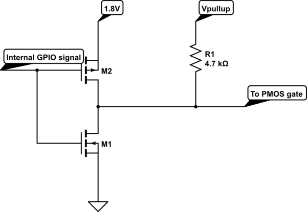
The output is very likely a push pull stage which has a (relatively) low output resistance.
What you effectively have is this (assuming you are using a CMOS device)

simulate this circuit – Schematic created using CircuitLab
The output when high will have M2 on and M1 off.
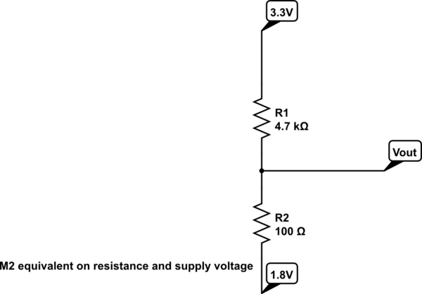
The output of this stage when high will have a typical resistance to 1.8V of perhaps a few tens (sometimes higher) of ohms; the voltage divider formed of M2 and the pullup resistor will maintain the output voltage at close to the GPIO drive voltage of 1.8V
You could use an open drain output but ensure it is safe to use with a 3.3V pullup (that will be in the datasheet).
The effective circuit in the high output state is this:

From the voltage divider principle, the voltage at Vout will be 1.83125V (assuming the on resistance of M2 is 100 ohms).
You should not normally pull a push pull / totem pole output beyond its supply voltages whether that be positive or negative.
-
\$\begingroup\$ can you please elaborate how the divider formed will maintain 1.8 V at output and can you suggest me any articles to gain knowledge regarding these subjects. \$\endgroup\$ Commented Oct 18, 2019 at 12:57
-
\$\begingroup\$ @VigneshC Answer updated with equivalent circuit. \$\endgroup\$ Commented Oct 18, 2019 at 13:07
