7
\$\begingroup\$

I'm trying to understand what is the use of tri-state output and what is the advantage of using it.

Below depicts both two-state and tri-state output:

enter image description here

According to the above logic, it seems to me two-state output can only be ON or OFF. But in tri-state case, the output can be ON, OFF or floating. So to me the only difference is the floating state.

As far as I read, floating signals are not useful. But it seems I'm ignorant at some points and want to ask what is the purpose of using tri-state output?

\$\endgroup\$
1
  • 3
    \$\begingroup\$ Having a high impedance output allows the output to be driven by another device/elsewhere in the circuit \$\endgroup\$ Commented Nov 11, 2019 at 12:27

4 Answers 4

8
\$\begingroup\$

Tri-state is essentially 3 different states as you have seen. Instead of calling it ON and OFF, think of it as IN and OUT instead. The third state is not floating, it is in a high impedance state, which is essentially disconnecting it from the circuit. This means your 3 states are:

  • Input
  • Output
  • High Impedance (disconnected)

This is very useful in circuits that have a common bus for multiple components. With tri-state logic, components can either read from the bus, write to the bus, or be essentially disconnected so that it does not affect the bus, and will not be affected by the state of the bus either.

As an example of using tri-state logic is on a computer bus:

enter image description here

(Picture taken from http://www.lisbdnet.com/system-bus-functions-features/)

As you can see, multiple units are sharing the same busses. You don't want the information on the bus to be read by every unit at the same time. You also dont want them writing to the bus at the same time. With Tri-state logic, each individual unit can either read from the bus, write to the bus or just be disconnected. In this way, data can be sent back and forth and only the units that require the information will receive it. Imagine, with the above diagram, you receive an input to access a memory address, which then needs to be sent to a register, then go through the ALU, and finally the data is sent to the output. This can be done easily by changing the between the 3 states, so only the units that are needed will be connected to the bus at any time.

\$\endgroup\$
6
  • \$\begingroup\$ "... or be disconnected and be unaffected by it" ... and to "unaffect" the bus so that effectively that component is no longer in-circuit. \$\endgroup\$
    – Transistor
    Commented Nov 11, 2019 at 12:44
  • \$\begingroup\$ @Transistor good point, I'll add that in there! \$\endgroup\$
    – MCG
    Commented Nov 11, 2019 at 13:00
  • 1
    \$\begingroup\$ @MCG You mean ON is INPUT and OFF is OUTPUT? Why do you call them as input and output? Aren't all states output? Here they call them output i.sstatic.net/LutlM.png Could you clarify that as well? And if possible where in practice is this tri state used? Can we name any ? \$\endgroup\$
    – user1999
    Commented Nov 11, 2019 at 13:10
  • \$\begingroup\$ @user1999 It depends what you have connected to it, whether it is On/Off or Input/Output. It depends on the application. There isn't much advantage to a tri-state ON/OFF switch. As for inputs and outputs, I'll add an example to the answer \$\endgroup\$
    – MCG
    Commented Nov 11, 2019 at 13:46
  • \$\begingroup\$ "You don't want the information on the bus to be read by every unit at the same time" But this is what tri-state buffers actually lead to. Because the three states are "Output Low, Output High, and Input". Removing loads from the bus is valuable, but has little to do with "tri-state output", the topic of the question. \$\endgroup\$
    – Ben Voigt
    Commented Nov 6, 2023 at 16:59
4
\$\begingroup\$

Suppose that instead of just one switch you have many switches connected to the same tristate wire. That single wire can be used by all of these different switches to communicate information, as long as only one switch at a time uses the wire by connecting to '1' or '0'. By using just one wire for all of the switches, rather than a separate wire from every switch to every other switch, we can greatly reduce the amount of physical wiring needed.

This kind of situation occurs in practice when you want to connect a processor to different memory and I/O devices. The processor only talks to one of them at a time, so the wires used for communication (the data bus) are shared. Of course, the processor must have some mechanism for specifying which device is allowed to use the wires at any point in time...that is usually done with a separate set of wires (the address bus and a handful of control signals) that is one-way from the processor to the devices.

\$\endgroup\$
1
\$\begingroup\$

Before TriState logic/bus_drivers appeared, logic systems used multiplexors (ORs of ANDs) or wired_ORs.

The wired_ORs depended on resistive pullups, and were slow.

National Semi provided additional on_silicon transistors (using all NPN, the fastest cheapest silicon of that time) to disable both low_side and high_side driver of the TTL gate output circuits.

\$\endgroup\$
1
\$\begingroup\$

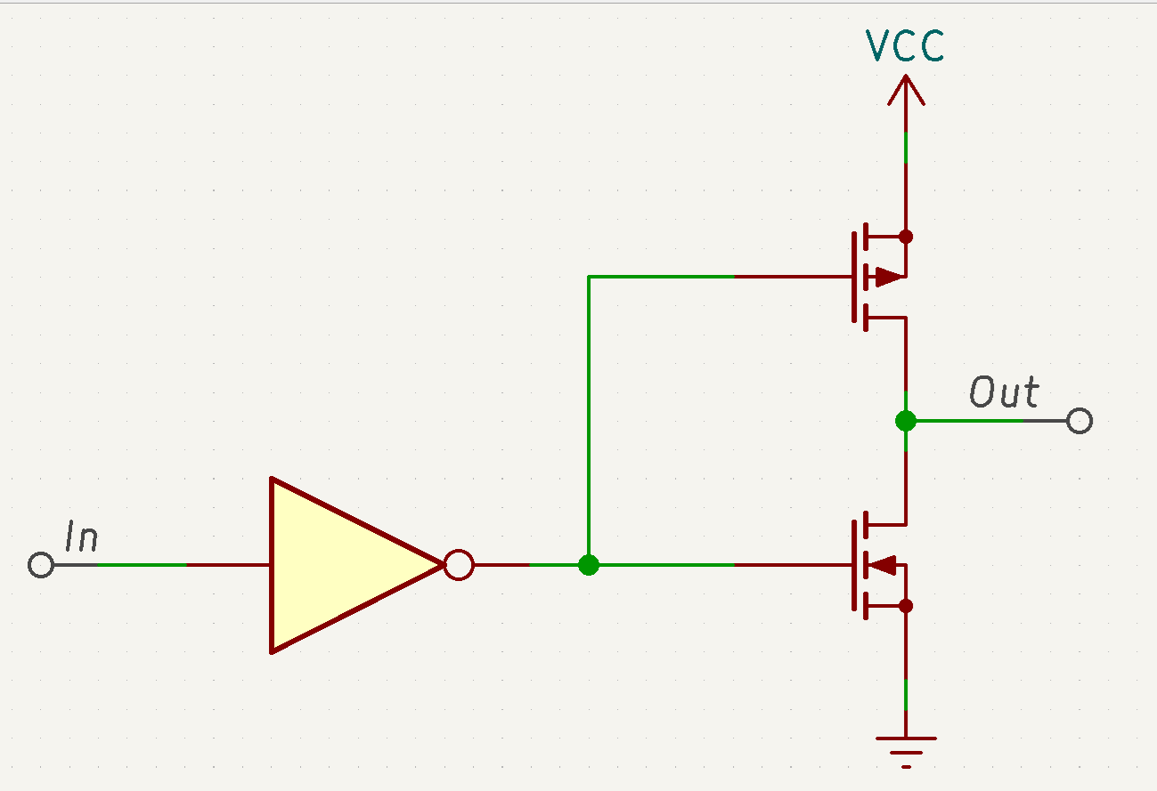
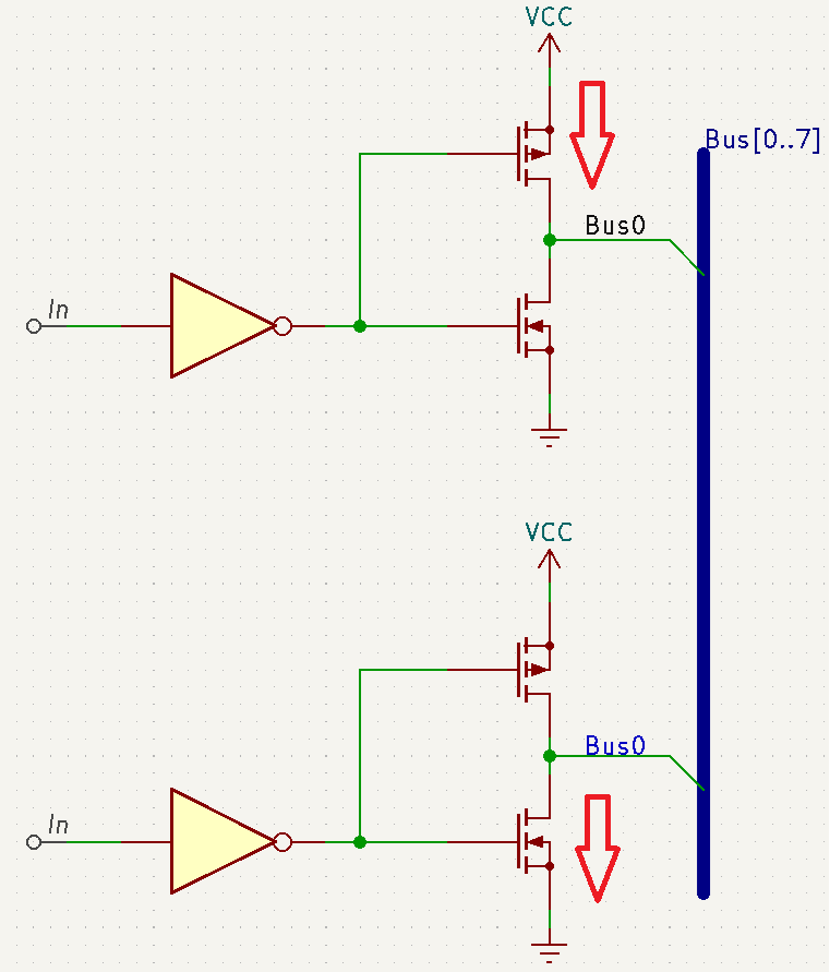
Your two state output is close but not quite to the point. The following (simplified) diagram shows the problem that a two state output could cause.

enter image description here

Imagine you want to connect to signal sources to the same bus. If you were to use simple two state logic. The moment one of the output goes high and the other goes low, you will have a shoot-through short-circuit because of the fact that the transistor of one output will be connecting the bus to Vcc and the transistor of the other one to GND.

enter image description here

In tri-state, the enable input allows the output to be completely isolated from the bus, preventing two outputs driving the bus to different states at the same time and causing device destruction

enter image description here

\$\endgroup\$
4
  • \$\begingroup\$ Your final diagram uses switches to float transistor base (or gate for FET). That's not right. If using a switch, it would go on the output side of the push-pull driver (and that's diagrammed wrong too, since it should pair one PNP and one NPN instead of two NPN). However, what's actually done is to control the base (or gate) to turn both push and pull transistors off, but that requires strongly driving their base into the desired state, not floating. \$\endgroup\$
    – Ben Voigt
    Commented Nov 6, 2023 at 17:03
  • \$\begingroup\$ @Ben. You're right correctness is important \$\endgroup\$
    – Krauss
    Commented Nov 7, 2023 at 13:01
  • \$\begingroup\$ All your diagrams have the PMOS transistors upside down. The source should go towards Vcc. \$\endgroup\$
    – Hearth
    Commented Nov 7, 2023 at 14:27
  • \$\begingroup\$ Thanks @Heart. This time it should work. \$\endgroup\$
    – Krauss
    Commented Nov 7, 2023 at 19:54

Your Answer

By clicking “Post Your Answer”, you agree to our terms of service and acknowledge you have read our privacy policy.

Not the answer you're looking for? Browse other questions tagged or ask your own question.