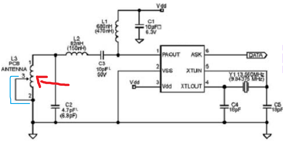
You don't choose a value for L3. It is a specifically shaped trace on your PCB.
The circuit you gave is a "typical application," but isn't a full design.
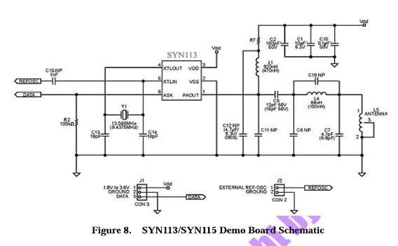
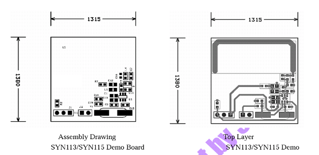
Later in the datasheet, the manufacturer shows the circuit and layout for a demo board they produce using the SYN115.
Here's the circuit:

Here's the layout:

L5 is the antenna in the schematic, and L5 is that thick trace along top half of the layout on the right (the top layer.)
The parts list also says that L5 is the antenna and that is part of the PCB:

It is formed and dimensioned to be resonant at the transmitter operating frequency of the transmitter.
There are no details given for the dimensions of L5.
You have a few options:
- Contact the manufacturer and ask for more details.
- Place a jack for an antenna connector and use a normal antenna.
- "Eyeball" the dimensions of the example antenna and hope for the best.
If you work for a company that will be making a whole bunch of these things, then you should go with option 1. Options 2 and 3 are really only "usable" if you are doing a one off for a hobby project.
Another option would be to study antenna design, and design your own loop antenna and matching network.
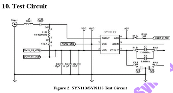
If you'd like to install a jack and connect a regular antenna to the chip, then have a look at Figure 2 from the datasheet. That's a test circuit followed by a PCB layout. It includes a circuit for connecting a 50 ohm antenna jack.

As a final option, you can just ignore matching and antenna design and just do what all the manufacturers do that make and sell the cheap SYN115 modules on AliExpress: Include an eyelet where the antenna should be (the antenna jack in Figure 2) and just hang a random piece of wire on it as an antenna.
Most of the projects you'll find on the internet that use these modules don't even bother putting an antenna wire on the module. They just assume (as you seem to) that the modules have an antenna on board.

