14
\$\begingroup\$

STM32F446xC Power Scheme

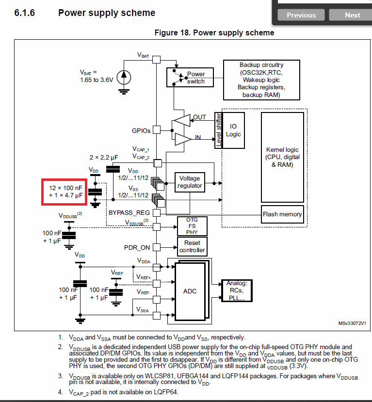
I am learning to make my first PCB with an MCU and looking at the Power Scheme, it asks for 12 x 100nF capacitors. My question is why have 12 of them rather than 1 x 1uF, and 2 x 100nF (I see that there is limited value selection, but these are popular values too)? This would save space, and manufacturing costs. I also assume these are in parallel to add up the capacitance, is this a wrong assumption? Thank you for your help.

EDIT:Thank you for all the good advice, due to request, here is the datasheet: STM32F446xC Datasheet

\$\endgroup\$
6
  • 7
    \$\begingroup\$ It's not only the capacitance, but also the inductance of the PCB trace. The bypass capacitors really do need to be close to the IC to do any good, and each should have its own route to the corresponding IC pins. Where there are fast rising/falling edges (like fast digital signals) think of each PCB trace as a resistor and an inductor. \$\endgroup\$
    – MarkU
    Commented Jul 15, 2020 at 6:41
  • 2
    \$\begingroup\$ Will - Welcome :-) FYI this is a previous (answered) question on the same topic (multiple decoupling capacitors recommended for MCUs): "Multiple identical parallel capacitors" \$\endgroup\$
    – SamGibson
    Commented Jul 15, 2020 at 12:42
  • \$\begingroup\$ For PCB layout, look at the layout advice section of the datasheet. The manufacturer should tell you exactly where all those capacitors belong. That's the critical thing. \$\endgroup\$
    – John Doty
    Commented Jul 15, 2020 at 21:22
  • 1
    \$\begingroup\$ @Will Can you add a link to that datasheet please? (Partly because I'm interested in seeing the original, partly because it's good manners to mention the source when you quote some document.) \$\endgroup\$
    – ilkkachu
    Commented Jul 16, 2020 at 9:56
  • 2
    \$\begingroup\$ See this related question and its answers. Also, for general background on these caps, please see this one, too. \$\endgroup\$
    – bitsmack
    Commented Jul 16, 2020 at 10:55

4 Answers 4

46
\$\begingroup\$

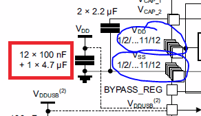
Because the chip has 12 (maybe depending on the package) pairs of Vdd and Vss pins. Each pair should get its own decoupling cap.

enter image description here

\$\endgroup\$
1
  • 4
    \$\begingroup\$ The fact that the Vdd and Vss pins are also drawn as stacks of squares hints that it's not one pin, but several. Just above there's Vcap_1 and Vcap_2, with a double square on the pin and "2 x 2.2 uF" next to the cap. \$\endgroup\$
    – ilkkachu
    Commented Jul 16, 2020 at 9:26
17
\$\begingroup\$

Each of your decoupling capacitors exists to provide current when the load (your MCU) switches and needs more current very quickly. The power supply takes time to respond to this transient demand and increase its current output to stop the supply rail falling. The connections to the power supply have an impedance that also slows its response to the load. So you have decoupling capacitors that supply these fast transient currents as needed when MCU switching occurs, charging back up when during steady load times.

A capacitor has a capacitance value and, among other characteristics, an Equivalent Series Resistance (ESR) value which is specified at some frequency of operation. The ESR can be seen as a resistance in series with the capacitor.

Using 12 x 100 nF capacitors in parallel and placed closely together instead of 1 x '1200 nF' capacitor would give the same capacitance but with a lower ESR because all the 12 capacitor ESRs are in parallel with each other. It doesn't give an overall 12th of a single capacitor's ESR, because the interconnecting PCB tracks have an impedance, but it's much lower than the ESR of a single capacitor.

Here, your MCU recommends placing a capacitor near to each of many (12?) MCU supply pins. Each supply pin now sees a nearby capacitor with a lower ESR (and therefore a faster transient current response) than if it was one larger capacitor shared between them.

\$\endgroup\$
3
\$\begingroup\$

To add to the good answers already here: you can replace multiple capacitors in parallel by one with the sum of their capacitance only if you can neglect the resistance and inductance of the wires that connect them. At high frequencies, the inductance of wires in particular becomes harder to neglect, so you cannot do that.

\$\endgroup\$
1
  • 6
    \$\begingroup\$ Correct, of course. Just a word of caution in case someone reads it the wrong way for this particular case: in the OP's case you cannot neglect the trace effects, and they must be placed directly at the Vss/Vdd pins: "12x" is a hint to layout. \$\endgroup\$
    – P2000
    Commented Jul 15, 2020 at 15:12
2
\$\begingroup\$

Beware though of the parasitic R and L of capacitors. Here we have 12 X 100n in parallel with 1X 4.7u If the capacitors are ideal there would be no need for the 12 X 100n

In fact the 4.7uF will have significant self inductance and so have high impedance above a few MHz, The 100nF are there to provide low impedance up to higher frequencies. A 1200nF will be worse at those frequencies. It's not uncommon to put a 10nF in parallel with a 100nF to provide good decoupling up to the GHz range. 10nF caps are available with better dielectrics so they have lower parasitics, but you can't fit much capacitance in the same size package.

Also as others have said keep the track to the power pin and ground short or the cap has no effect.

Alway check the datasheets; https://www.farnell.com/datasheets/2167237.pdf

Building circuits is always a bit harder than just the schematic, but it does make for an interesting job.

\$\endgroup\$

Not the answer you're looking for? Browse other questions tagged or ask your own question.