2
\$\begingroup\$

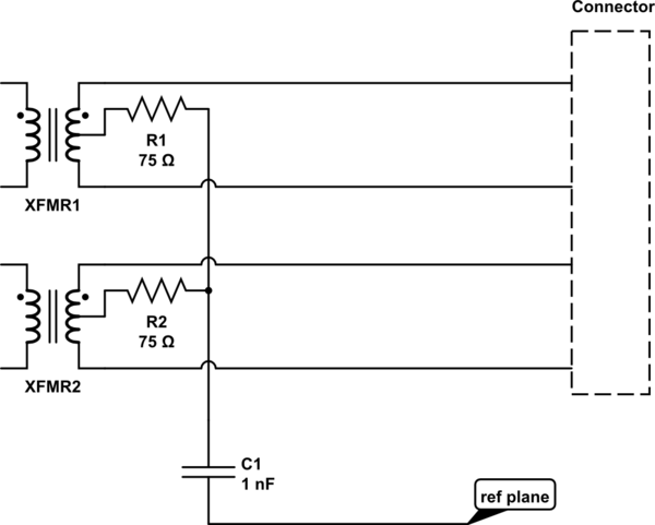
I am routing a flexible PCB which connects a panel-mount ethernet connector (without integrated magnetics) to a rigid PCB which contains the ethernet magnetics. I plan to route the differential pairs as edge-coupled microstrips (100ohm differential impedance). The reference plane that I'm routing the traces over is connected to Bob Smith termination as shown in the diagram.
schematic

simulate this circuit – Schematic created using CircuitLab For simplicity I have shown only two of the data pairs and omitted the common-mode chokes.

I have some doubts over whether my edge coupled microstrip will give me the expected differential impedance. I can use field solvers to determine the necessary trace width/space for my stack-up. The results I get show that most of the coupling is to the reference plane beneath the traces (Z0) rather than directly between traces (Zcoupling). But because my connector has no "ground" pin to connect to the reference plane, I don't understand how any return currents can possibly flow through this plane? Would this make my calculated differential impedance invalid?

\$\endgroup\$

1 Answer 1

1
\$\begingroup\$

But because my connector has no "ground" pin to connect to the reference plane, I don't understand how any return currents can possibly flow through this plane?

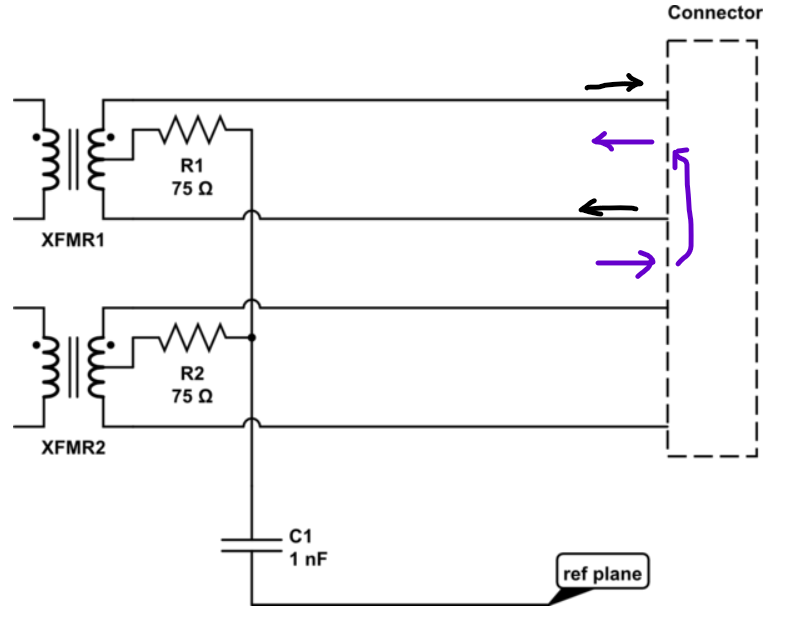
Think about the relationship between the return currents under the two signal traces. Here I've given an example with the signal currents indicated in black and the return currents in blue:

enter image description here

Since the return currents for the two conductors of the differential pair are in opposite directions, there's no need for any current to flow into the the connector. The return current can simply circulate from the region under one signal conductor to the region under the other.

That said, there will of course be a slight field discontinuity due to the change in geometry between the PCB traces and whatever the structure is inside the connector. You'll want to be sure you're following the manufacturer's advice on the PCB footprint, keep the distance between the magnetics and the connector short, etc., to minimize the effect of this discontinuity. But if you do that, it's likely the discontinuity won't adversely affect your design. If it does, the problem is more likely to manifest in a radiated emissions violation rather than a performance problem.

\$\endgroup\$
1
  • \$\begingroup\$ Good answer thanks. You say shortening the distance between the magnetics and connector will minimize the effect of the discontinuity. Could you explain why? My guess is that the magnitude of the discontinuity (and resulting reflections) will be the same. But it will somehow have less impact because it is nearer to the end of the transmission line. Is this correct? \$\endgroup\$
    – Nick
    Commented Jun 21, 2021 at 7:25

Your Answer

By clicking “Post Your Answer”, you agree to our terms of service and acknowledge you have read our privacy policy.

Not the answer you're looking for? Browse other questions tagged or ask your own question.