5
\$\begingroup\$

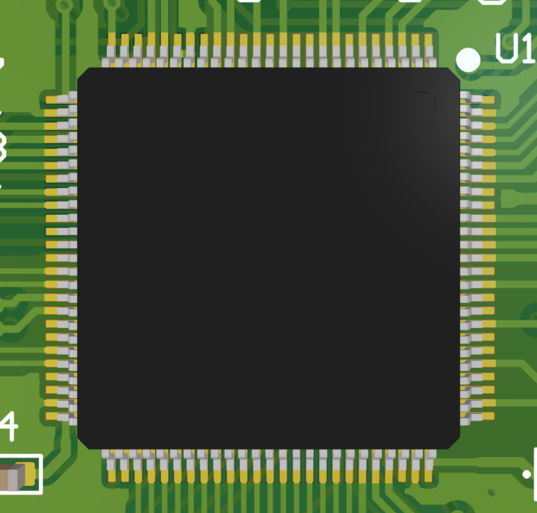
Considering we're designing a two-layer PCB with a 100-pin MCU, what's the best way to routing? As you can see in the image, many pins of this MCU are used (almost all.)

enter image description here

When designing a two-layer PCB, I think it is the most logical way to use the bottom as the GND plane and the top as the SIG/PWR. I know I can draw small tracks without disturbing the GND plane too much.

Unfortunately, I don't have enough space on the top layer for the tracks because too many pins are used. I therefore have to draw as many tracks on the bottom layer as I have on the top layer. It's impossible for the bottom GND plane to stay in one piece.

In this case, is it a good practice to pour GND to the top and bottom layer?

\$\endgroup\$
1
  • 7
    \$\begingroup\$ Not a full answer, but I find rotating QFN/QFP packages by 45 degress helps with routing. \$\endgroup\$ Commented Dec 30, 2022 at 14:29

3 Answers 3

27
\$\begingroup\$

If you really are stuck with 2 layers, then you need to be systematic, otherwise you don't have a chance. Use Manhattan routing, East-West tracks on one layer, North-South on the other, predominantly at least. Then you can route from anywhere to anywhere, using vias to change direction as required, and only moving tracks a little if there's congestion, rather than ripping up and re-routing.

Make the first tracks you put in a grid of grounds, so a track every 10 mm on each layer in the appropriate direction, via'd through at each intersection. This will give you something almost as good as a ground plane. Then place your supply decoupling components close to the IC. Then route high speed tracks next to the ground traces. Then route the rest. Don't succumb to the temptation to put in a ground fill thinking that will solve your grounding problems. All it will do (with 2 layers) is to make it more difficult to see whether all high speed signals have their close ground trace. With 4 layers you do have the space to use a ground plane

However, the cost of a 4 layer board is so close to that of a 2 layer (an assembled, tested, manufactured board, not just the bare board), and the cost of the extra time needed for designing, debugging, and reworking a board constrained to 2 layers is so high (including the cost of getting to market later), that you really ought to push back on this short-sighted requirement.

To be fair, there is one benefit of a 2 layer board, and that is, all tracks are on the surface. This makes rework simpler in some cases where you might want to cut or bridge tracks. However, it's a small benefit to weigh against the other large costs.

A good metric for PCBs is fractional component area - how much of the board area is component footprints, and how much is track. Perform that sum quickly for a few of your company's recent boards. A 2 layer design will require a bigger board, because all of those tracks have to be on the surface. Will the bigger board fit in your enclosure? What's the cost of a bigger board that's cheaper per square cm, compared to a smaller board?

I've lost count of how many times in my long career that the edict has come down from on high that we'll do it this cheap way, and it's ended up costing us far more (especially time to market) because only some of the costs of the different methods were compared.

\$\endgroup\$
2
  • 2
    \$\begingroup\$ +1 for the last paragraph alone. I've spent weeks of work only to save a few £s on a 2 layer board \$\endgroup\$
    – D Duck
    Commented Dec 31, 2022 at 14:01
  • 1
    \$\begingroup\$ At one point, my company asked me to do a design. I took one look, and at the few we'd done recently, and insisted on 8 layers. They grumbled for a bit, then acquiesced, and the design was done easily, quickly, and evolved when (don't you just know it!) new requirements were added late into the project. \$\endgroup\$
    – Neil_UK
    Commented Dec 31, 2022 at 15:29
10
\$\begingroup\$

When designing a two-layer PCB, I think it is the most logical way to use the bottom as the GND plane and the top as the SIG/PWR. I know I can draw small tracks without disturbing the GND plane too much.

Yes, that's how I'd do it.

However, I don't have enough space on the top layer for the tracks because too many pins are used. Therefore, I have to draw as many tracks on the bottom layer as I have on the top layer. It's impossible for the bottom GND plane to stay in one piece.

Time to consider using a 4 layer PCB.


Added section on making a case for a more expensive 4-layer design

Part of an engineer's job is to sometimes justify a more expensive component. In this case it's simply going from a fairly difficult (and apparently cheaper) double-layer PCB to a much easier to design 4-layer PCB. But, there's more to it than this; if the circuit on 2-layers underperforms (due to noise or EMI reasons) then some customers will be disappointed <-- how much extra cost should you embed into a product to avoid customer disappointment?

If the 2-layer circuit has a higher failure rate in test then this means money down the drain. Maybe it might also take longer to test? Maybe it might take longer to build? Maybe the component placement (to aid a 2-layer design) compromises its ability to be mounted correctly <-- this might lead to other problems that ultimately represent a hidden cost.

Maybe the field failure rate might be higher with a compromised design? Again this can lead to customer disappointment and what price do you place on customer disappointment?

What if you have to evolve the design at some later stage? Will this be accomplished so easily with a "busy" 2-layer design or, will a "more simple" layout using 4-layers make this easier?

\$\endgroup\$
12
  • 2
    \$\begingroup\$ Does it need to pass EMC regulations? Does it need to be a resilient design? Is noise an issue? Is the presence of other tech an issue? If no to all 4 then build as a 2 layer PCB. \$\endgroup\$
    – Andy aka
    Commented Dec 30, 2022 at 10:33
  • 4
    \$\begingroup\$ You will probably fail the EMC with two layers PCB. \$\endgroup\$
    – Vincent
    Commented Dec 30, 2022 at 10:33
  • 7
    \$\begingroup\$ Your stingy company is likely to pay more in the end due to the difficulties and problems likely to arise with a 2 layer layout. 4 layer boards are so cheap nowadays that it's almost a no brainer for anything beyond the most basic digital designs. \$\endgroup\$
    – TypeIA
    Commented Dec 30, 2022 at 10:35
  • 2
    \$\begingroup\$ If you are happy to pay for the consequences of using a 2 layer board later then that is your, or your company's, choice - affects the profit though. The 5 P plan: Proper Planning Prevents Poor Performance. \$\endgroup\$
    – Solar Mike
    Commented Dec 30, 2022 at 10:54
  • 3
    \$\begingroup\$ @harmonica If the time and money spent getting a 2 layer design done into a working sellable product exceeds the time and money to make a 4 layer design then they should care. \$\endgroup\$
    – Justme
    Commented Dec 30, 2022 at 11:01
8
\$\begingroup\$

Using the bottom layer as GND plane is only possible for the simplest circuits due to congestion as you have noticed.

You can go a bit further if you abandon the idea of a ground plane for 2-layer boards, and instead just make sure that every high speed current has a tight deliberate return current path.

Such designs can be made to pass EMc testing, but require tons more effort than just using ground planes in a 4 layer board. Therefore, the 2-layer board is only really worth it if you plan on making 1000s of board each of which would sell for a tiny price.

\$\endgroup\$
6
  • 1
    \$\begingroup\$ About 1000 PCBs will be sold annually. That's why they try to reduce the cost as much as possible. \$\endgroup\$
    – harmonica
    Commented Dec 30, 2022 at 11:59
  • 2
    \$\begingroup\$ @harmonica what’s the failure or return rate on those 1000? That could be more useful… \$\endgroup\$
    – Solar Mike
    Commented Dec 30, 2022 at 12:07
  • 2
    \$\begingroup\$ @SolarMike Currently, old PCBs that I did not design are selling(2-layer), and the number of PCBs fail and come back to our company is very high \$\endgroup\$
    – harmonica
    Commented Dec 30, 2022 at 13:51
  • 3
    \$\begingroup\$ @harmonica so spend the money to deal with returns and make sure to create more by sticking with a 2 layer board. \$\endgroup\$
    – Solar Mike
    Commented Dec 30, 2022 at 15:43
  • 3
    \$\begingroup\$ For reference, computers in the 80s were regularly made in 2 layers, no ground plane -- signal quality wasn't an issue because TTL/CMOS was slow (clock rate of a few MHz). They clamped the board in metal shields to pass EMC. This is not possible today, with even mere signal quality being inadequate with 20MHz+ MCUs. If you want to avoid the cost of shields, a ground plane is mandatory, and either enough routing area to pour a contiguous plane, or enough layers to resolve routing while keeping at least one solid plane (preferably two). \$\endgroup\$ Commented Dec 30, 2022 at 15:51

Your Answer

By clicking “Post Your Answer”, you agree to our terms of service and acknowledge you have read our privacy policy.

Not the answer you're looking for? Browse other questions tagged or ask your own question.