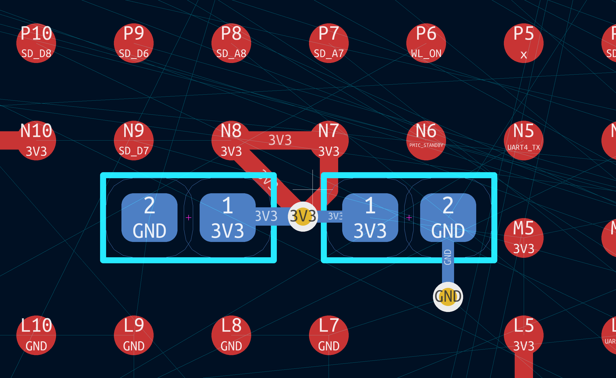
Here is what I am wondering. Is the example PCB layout fine for handling bypass capacitors? Or, do I need to run a separate VIA as well? Note that the blue caps are on the backside of the PCB.
Also, I understand that this layout is incomplete, I'm just curious about the shared via. :-)

