0
\$\begingroup\$

I am designing an RF amplifier (< 13 GHz) and want to use a board with two layers. However, the RFIC footprint (16-VFQFN Exposed Pad) has RFIN on the left, VDD on top, RFOUT on the right, and VGG on the bottom side, see the schematic symbol.enter image description here
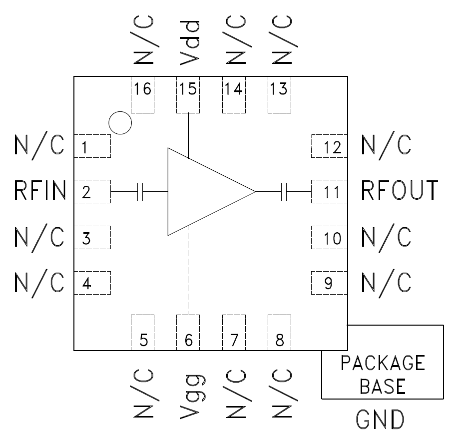
My feeding network will be above the VDD pin. All N/C pins are connected to the GND. The package has an exposed pad also connected to GND. Both layers will be filled with GND.

Considering the outlined case, can I route the VGG signal on the bottom layer under the RFIC?

\$\endgroup\$
2
  • \$\begingroup\$ What is the part number of the RFIC, and does the manufacturer provide a recommended layout? \$\endgroup\$ Commented Sep 30, 2023 at 15:23
  • \$\begingroup\$ @ChesterGillon, the manufacturer provides recommended layout. However, it is simplified to a version where the Vdd and Vgg are connected to pins, and no further feeding network is employed on the PCB. There is a link to part: analog.com/media/en/technical-documentation/data-sheets/… (the picture in the post above is a simplified schematic symbol, as Vgg1 = Vgg2, if I understood the datasheet correctly). \$\endgroup\$ Commented Sep 30, 2023 at 15:28

0

Your Answer

By clicking “Post Your Answer”, you agree to our terms of service and acknowledge you have read our privacy policy.

Browse other questions tagged or ask your own question.