1
\$\begingroup\$

I came across this post on how to reduce EMI in a PCB. From this, I learned that there actually exist two types of current. The first is the conductive current (the current that flows through a conductor) and the second is magic (or displacement current). This displacement current is 99.9999999% the reason why electronics is considered black magic :).

In the post they show that it is best to use smaller traces for high frequency is a must! From Maxwell's equations:

enter image description here

The contribution from Maxwell is the second term in the parentheses, this term explains how much displacement current will exist.

Basically having a smaller conductive area, reduces this term and thus the magnetic field created for high-speed signals. Hence reducing unwanted EMI emissions and interference with neighboring tracks.

The post included this picture: enter image description here
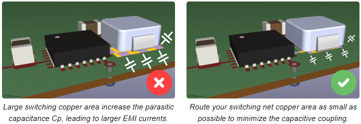
Please see link here

My questions:

  1. Is what I explained above correct?

  2. I know that adding a ground plane to the bottom layer of the PCB helps with EMI, however, how does it help exactly? I am assuming is reduces the capacitance, but how does it reduce it?

\$\endgroup\$
2
  • \$\begingroup\$ What do you mean by "adding ground plane"? Would there not be one on inner layers already? | There are a variety of considerations where plane use and trace width matter, and best geometry varies for many reasons; a clearer answer will be possible if you can define a particular case. The picture seems to suggest SMPS, but it's not clear from the text if that is your concern. \$\endgroup\$ Commented Oct 21, 2023 at 18:45
  • \$\begingroup\$ @TimWilliams I have added the link. This is for a SMPS application \$\endgroup\$
    – JoeyB
    Commented Oct 21, 2023 at 21:28

1 Answer 1

2
\$\begingroup\$

Is what I explained above correct?

I don't think you really need to bring any of Maxwell's equations into this.

It helps both electric field problems and, it helps magnetic field problems. As a large piece of copper, the ground-plane acts like a shield and diverts electric field interference to a safe place rather than hit sensitive nodes.

Magnetically, when a high speed signal is transmitted from one chip to another there will be an associated high-speed current. That's the forward path but, the return path from the receiving chip back to the sending chip is also a high-speed current. Without a ground-plane the forward and return PCB tracks form a loop that will emit EMI. If you are skilled you can stack forward and return tracks on top of each other and minimize the EMI loop size.

That's also why we use specialist cables like coax and twisted pair.

However, with a ground-plane, the return current naturally flows underneath the forward current track and this automatically minimizes the EMI loop size.

\$\endgroup\$
2
  • \$\begingroup\$ Thanks Andy, I just wanted to understand what my 4 years at uni was for :). Hence I wanted to tie the theory with practical electronics. \$\endgroup\$
    – JoeyB
    Commented Oct 21, 2023 at 17:40
  • 1
    \$\begingroup\$ @JoeyB are we done now or do you still need information? \$\endgroup\$
    – Andy aka
    Commented Oct 31, 2023 at 12:32

Your Answer

By clicking “Post Your Answer”, you agree to our terms of service and acknowledge you have read our privacy policy.

Not the answer you're looking for? Browse other questions tagged or ask your own question.