1
\$\begingroup\$

I have a PCB where I use ECS-240-8-36CKM-TR3 crystal for ADUM4166 isolator and USB2517-JZX USB hub. My circuit works as expected and I want to see and check if the oscillation of the crystals is "fine". The problem is, I can not define "fine".

The reason behind the check I am making, is to justify the values and placement of the classic 1Mohm resistor across the crystal's Xtal1/Xtal2 pins, and the placement/values of the two capacitors on the crystals (I know how to calculate the capacito's value). I also want to see what "issues" the resistor fixes on the crystal's waveform versus what "issues" on the waveform the capacitor fix. (The before - after waveform after placing each component)

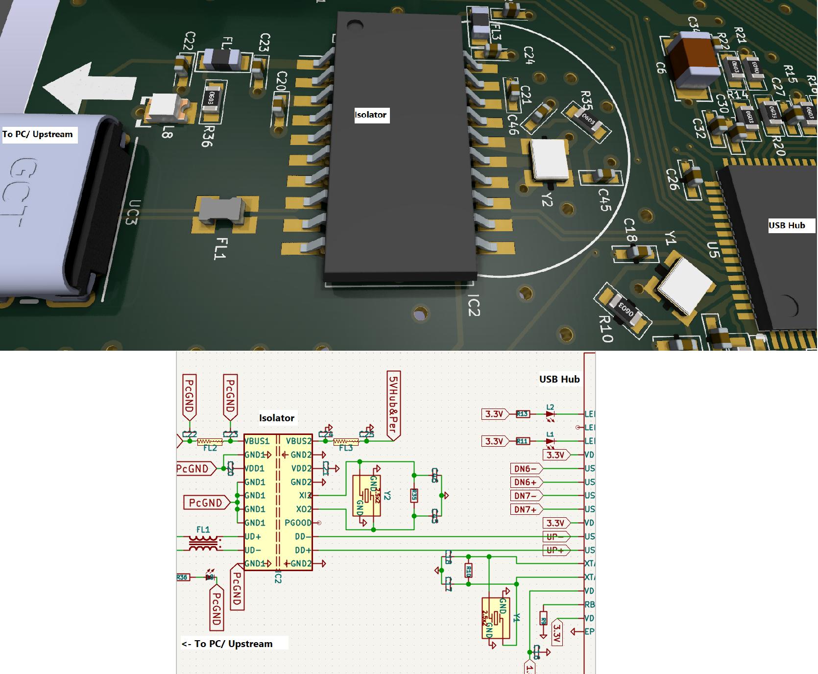
If the PCB layout/hookup matters, here it is:

My PCB hookup

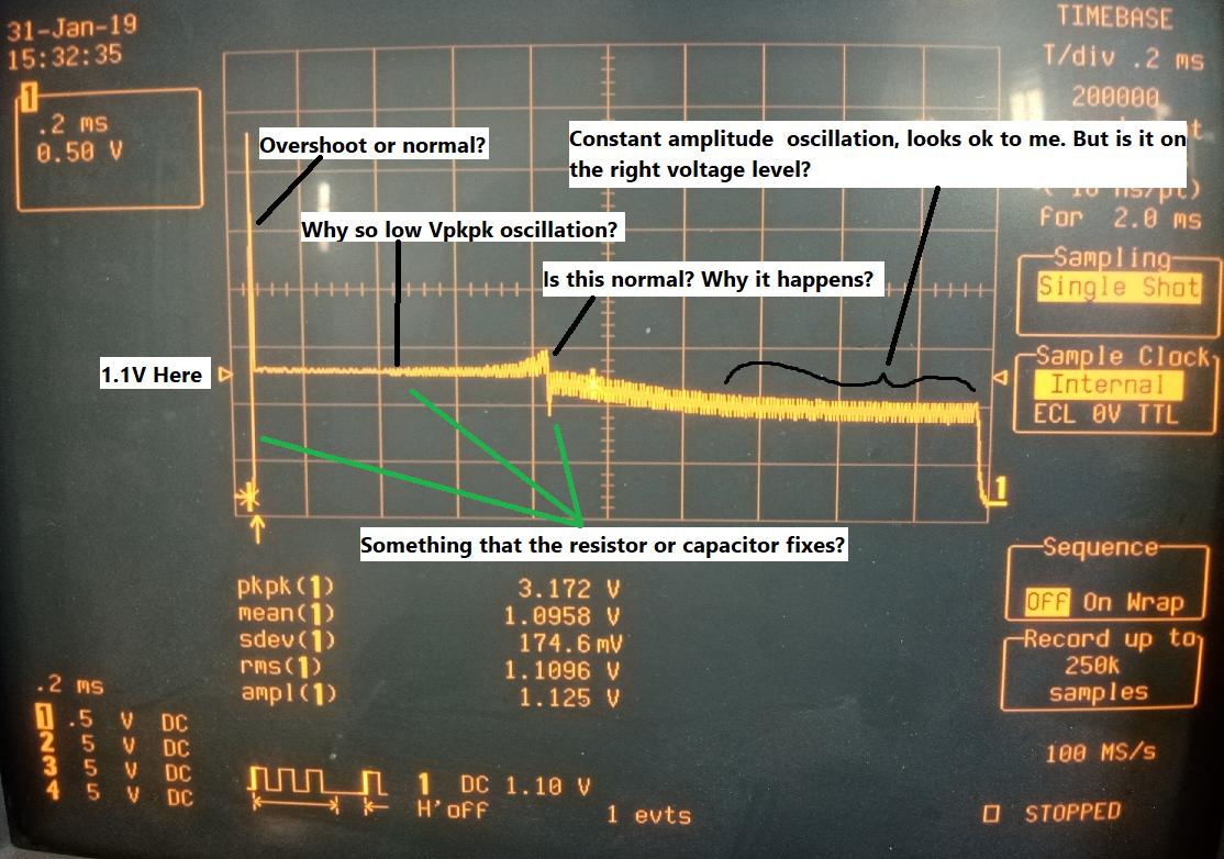
And here I probe one of the crystals under normal operation (the Isolator sends a signal to USB every couple of seconds and this waveform is shown on the crystal, it looks like the crystal starts, the isolator sends the signal, then the crystal shuts down):

Crystal waveform normal?

How should (I know) the startup/shutdown/normal operation voltage of each crystal's pin? The datasheets do not show the "Normal/nominal" crystal operation waveforms. Is there any manual for this purpose?

\$\endgroup\$
9
  • \$\begingroup\$ Any reason why component values aren't specified in the schematic? \$\endgroup\$
    – Lundin
    Commented Jan 5 at 15:22
  • \$\begingroup\$ @Lundin I specify them always in the BOM, but I guess I could specify them in the schematic :p . If I specify the values in both BOM and schematic, in case of a value change, I might forget to update the schematic or the BOM, so I just keep them in one place (the BOM). (I also always DIY the BOM, Im not happy with the automatic BOM export) \$\endgroup\$ Commented Jan 5 at 15:27
  • \$\begingroup\$ Data sheet shows Fig.21 missing oscillator bias resistor (your R35). Biasing of this oscillator is often internal, so that an external resistor is not needed. Data sheet seems unclear if external biasing resistor is required. It should be easy to try leaving R34 open-circuit, and monitor XO2 to see if it remain near half-Vdd2. Your probing seems to slow oscillator start up significantly, and any frequency you measure will be lower than un-probed frequency. Do heed answers suggesting very light coupling to the oscillator - probing these high-impedance oscillators is not easy. \$\endgroup\$
    – glen_geek
    Commented Jan 5 at 17:12
  • 1
    \$\begingroup\$ From comment down below: You measured with 1X probe? That might explain the weird behaviour. If you have a 10x probe, re-test and show the waveform. And, if you have a 10x probe, why do you even bother using a 1x probe at all? The rule of thumb is, never use a 1x probe unless you know what you are doing and why. It is unlikely that your generic 1x probe has even got enough bandwidth for measuring a 24 MHz signal. \$\endgroup\$
    – Justme
    Commented Jan 5 at 17:22
  • 1
    \$\begingroup\$ @ChristianidisVasilis The values depend on the exact IC and exact crystal. Sometimes with ICs you are only given a manufacturer example with a certain crystal and you don't know what liberties you have regarding any values. Sometimes ICs require or work best or simply is validated with a crystal with given specs so you have no guarantees if it works with widly different crystal. Anyway, 1x probe waveforms of 24 MHz crystals are useless. \$\endgroup\$
    – Justme
    Commented Jan 6 at 11:59

2 Answers 2

2
\$\begingroup\$

The reason behind the check I am making, is to justify the values and placement of the classic 1Mohm resistor across the crystal's Xtal1/Xtal2 pins, and the placement/values of the two capacitors on the crystals (I know how to calculate the capacitor's value). I also want to see what "issues" the resistor fixes on the crystal's waveform versus what "issues" on the waveform the capacitor fix.

The 1 MΩ resistor turns the inverting gate (inside the chip) into a linear amplifier. The resistor (sometimes 10 MΩ) applies negative feedback and, a normally-unsuitable and unbuffered-gate, becomes a decent analogue amplifier with inverting gain.

It doesn't really affect anything else.

Internally (inside the chip), the gate's output resistance plays an important role in creating an extra bit of phase shift to ensure that the crystal "sings" accurately. That resistor (in conjunction with the loading capacitor attached to that pin of the crystal), creates this extra phase shift.

And, because the inverter, crystal and loading capacitors become a high-Q linear circuit, the oscillation takes time to reach a steady-state value. This can be in the order of several micro-seconds to several milli-seconds.

The overshoot (in the question image) is just the activation of the gate (internally activated it seems) and, initially, the negative feedback due to the 1 MΩ resistor doesn't happen immediately so, the pin in the diagram "hits" the 3.3 volt rail then rapidly drops to around mid-rail.

\$\endgroup\$
1
\$\begingroup\$

You seem to have measured the crystal directly at the pin. This gives only good measurement results with a special oscilloscope probe with <1pF load capacitance. Most probes have ~15pF which is in the range of the quartz crystal's parallel caps and therefore detune the oscillation a lot.

To see if the crystal has enough "headroom" for oscillation, a common test is to introduce a series resistor in the oscillation loop at the driver output and increase the resistance until the crystal stops its oscillation, then relax the resistance to 10% of the value. This is a good practice that also avoids overdriving the crystal by the driver IC.

\$\endgroup\$
5
  • 1
    \$\begingroup\$ This part also specifies a load capacitance of 8pF so it is pickier than most crystals. \$\endgroup\$
    – Lundin
    Commented Jan 5 at 15:20
  • \$\begingroup\$ Yeah, I measured the crystal directly to the pin with x1 probe. When you say "a series resistor in the oscillation loop", can you make it stupid simple? One resistor pin goes to the Xtal1 pin and the other resistor pin goes to the Xtal2 pin, right? \$\endgroup\$ Commented Jan 5 at 15:23
  • \$\begingroup\$ No, the resistor has to go from XO2 of the IC to the crystal terminal (only one resistor!) \$\endgroup\$ Commented Jan 5 at 15:25
  • \$\begingroup\$ Interesting. I haven't heard using a resistor to lower the driver of the crystal. I would like to see a source/document of that technique if you have a link. Makes sense but also adds more questions to my mind :p . (In my question the resistor I mention I mean the one that goes between Xtal1 and Xtal2 of the crystal, I should edit the question to add that detail.) And you know what? Maybe the same technique can be used for the Resistor between Xtal1/Xtal2 pins, lower its value from maybe 2Mohms and see how the crystal behaves. \$\endgroup\$ Commented Jan 5 at 15:40
  • 1
    \$\begingroup\$ Here you can read a whitepaper about "oscillation safety factor" (registration required): jauch.com/en-INT/know_how/… \$\endgroup\$ Commented Jan 5 at 15:44

Your Answer

By clicking “Post Your Answer”, you agree to our terms of service and acknowledge you have read our privacy policy.

Not the answer you're looking for? Browse other questions tagged or ask your own question.