0
\$\begingroup\$

This is the first time I am making a high speed PCB so I am a bit unconfident. the ic I am talking about is this: FTDI232H

I have followed the schematic in the datasheet above and I have placed the capacitors and inductors close to the ic and I think I have given enough clearance to the traces.

I am planning to use a top layer polygon pour around the ic to make routing easier. Is this a better alternative to using vias?

edit: Should I just add an extra 1 or 2 layers and make one of them ground (just using 2 layers currently)?

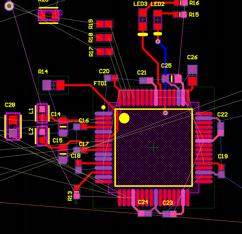
only using JTAG functionality and I have not forgotten oscillator and EEPROM

\$\endgroup\$
5
  • 1
    \$\begingroup\$ Without D+ and D- connected, the chip is not likely to do anything interesting :-) Seriously though... this particular chip is actually rather forgiving. I suggest you have a look at the Mini Module board layout as a reference design. \$\endgroup\$
    – TypeIA
    Commented Feb 9 at 14:01
  • 1
    \$\begingroup\$ Yeah I would expect to see the actual data lines since those are the critical ones. The general rule of thumb for RF design is to start with your most critical signals first then do the rest. It is probably not recommended to use vias if it can be avoided. And avoiding it will be easy if you start with the RF signals before anything else is routed. \$\endgroup\$
    – Lundin
    Commented Feb 9 at 14:16
  • \$\begingroup\$ I simply havent connected the USB lines (D+ and D-) to their circuitry, is USB the only thing that is considered high speed here? \$\endgroup\$
    – cr1tical1
    Commented Feb 9 at 14:34
  • \$\begingroup\$ How many layers you have now, 2? How long will USB travel on this PCB to some connector? How thick is the PCB, 1.6mm / 63 mils? The chip uses USB at 480 Mbps and capable of 12 Mbps baud rates. 480 Mbps USB means you need analog bandwidth far beyond GHz and it requires a 2 to 2.5 GHz oscilloscope to look at the waveforms. \$\endgroup\$
    – Justme
    Commented Feb 9 at 14:44
  • \$\begingroup\$ yep will need to move the USB stuff closer \$\endgroup\$
    – cr1tical1
    Commented Feb 9 at 15:14

2 Answers 2

0
\$\begingroup\$

First, I would determine what your PCB stackup is going to look like. Are you planning on doing 2-layers, 4-layers, etc? You might look at the PCB manufacturer and see if they have a simple 4-layer stackup you can reference and copy for example.

You can set up a diff pair directive in the schematic to assign a diff pair class if you have more than one type.

Then, in the Layer Stackup Manager, you can define an impedance profile. These are just starting points, you may need to update the width and trace spacing for something that's manufacturable.

enter image description here

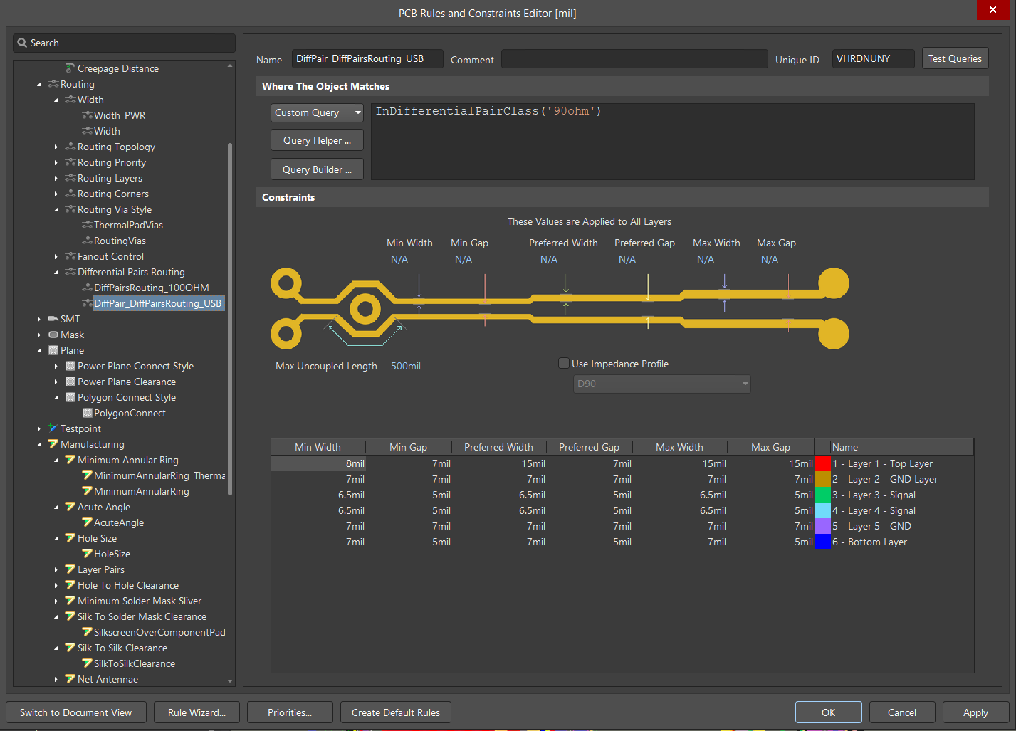
After doing that, you can create a design rule that uses the impedance profile and will point it to the diff pair class from your schematic. If you didn't have a diff pair class in your schematic, then the rule will just use 'All Differential Pairs' for the 'Diff Pair Class'.

enter image description here

Depending on what you're overall design looks like, you might not need to constrain your design like this. It's hard to tell though from the details provided.

\$\endgroup\$
0
\$\begingroup\$

If you are talking about USB2.0, then yes you will need to use a 90Ω differential pair transmission line. Try to keep the diff pairs on the same layer, you can use vias, if you do make sure the reference layer has the proper stackup (especially if it's an internal plane. Each diff pair needs a continuous reference plane if possible. Also make sure that the trace length does not approach 1/4λ wavelength which is 12" for 240MHz of USB2.0

As far as the UART side goes, it's probably not critical to worry about high speed on that side. Keep rise times low by minimizing capacitance and increasing inductance of traces.


Here is a better guide: https://e2e.ti.com/cfs-file/__key/communityserver-discussions-components-files/171/USB-2.0-Board-Design-and-Layout-Guidelines.pdf

\$\endgroup\$

Your Answer

By clicking “Post Your Answer”, you agree to our terms of service and acknowledge you have read our privacy policy.

Not the answer you're looking for? Browse other questions tagged or ask your own question.