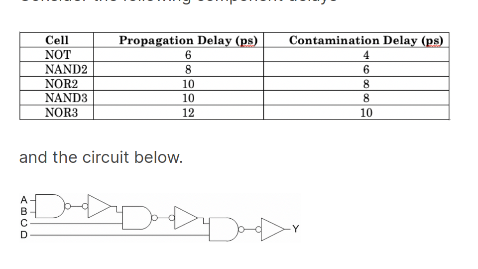
The problem is a homework problem from the EDX Digital Logic class. Please avoid looking at the rest of the post if you don't want to know the solution. I've already attempted the problem and know the solution because I got it wrong. I'm trying to understand the solution.
Consider the following circuit:

Based on the problem, the propagation delay is 42. Can we simplify the circuit to have a lower propagation delay?
I recognize that the "bubbles" can be canceled between the inverters and the NAND2 gates such that Y = ABCD (an AND4 gate)
The solution to the problem says you should be able to rewrite circuit with a propagation delay of 18. Can someone please explain how?
I've tried to convert the AND gates into OR gates with inverted inputs, but that doesn't work. Assuming the answer is correct, the only combination(s) that can get a propagation delay of 18 are:
1. 3 NOT gates which can't convert 4 inputs into 1 output
2. 1 NAND3 and 1 NAND2 (which leads to !(!(ABC)D) which isn't ABCD
3. 1 NOR2 and 1 NAND2 which can't convert 4 inputs into 1 output
and so forth
