2
\$\begingroup\$

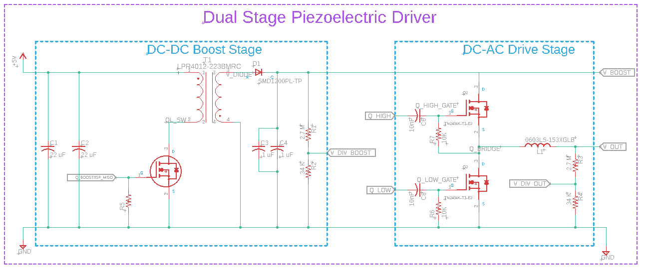
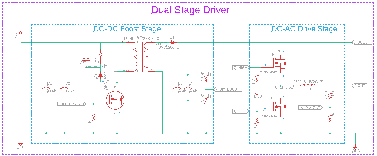
I'm working on a simple dual stage piezoelectric driver consisting of a DC-DC flyback converter (programmable from 50V to 250V) and a DC-AC half-bridge unipolar inverter. The flyback converter is working great!..But I'm having trouble with the DC-AC stage.

The DC-AC stage takes the high voltage DC generated by the flyback converter, and creates an arbitrary high voltage (0v to Vboost) at V_out when Q_high (increases voltage) and Q_low (decreases voltage) are pulsed on/off. Using a voltage divider for V_out feedback, I compare the output voltage to my desired reference waveform in my processor's memory and generate the necessary pulses to create the arbitrary waveform (Square, Triangle, Sinusoid, sawtooth etc.).

Currently Q_high gate is being driven by my MCU at 5V, which is obviously not high enough to produce the Vgs needed to keep the transistor on as Vout rises.

I've started reading up on gate drivers, and bootstrap circuits. The IRS20752LPBF Gate Driver grabbed my attention, but I'm concerned this device won't work when my load V_out voltage changes as a function of time.

So my question for everyone: what is a good method for controlling the high side MOSFET, given V_out is an AC (unipolar) waveform? And can I just use a gate driver in this application?

My Assumptions: I don't need a bootstrap circuit to control Q_high, since I am fine with keeping V_out 5V or more below V_boost. Second, I can't pull Q_high up to V_boost when I want to turn it on, and GND when off, since that will violate the maximum Vgs ratings; I need to be more clever and drive the gate with either V_out (off), or Vout + Vth (on).

Dual Stage DC-AC High Voltage Driver

\$\endgroup\$
10
  • \$\begingroup\$ Well despite your worries, the answer is still a high side driver. \$\endgroup\$
    – Andy aka
    Commented Aug 18, 2020 at 17:47
  • \$\begingroup\$ You could diode-clamp the gate to V_BOOST and drive it through a capacitor, if the Vgs parameter isn't exceeded. Then your 0 to 5V signal is V_BOOST-0.7 to V_BOOST+4.3. \$\endgroup\$ Commented Aug 18, 2020 at 18:16
  • \$\begingroup\$ @Andyaka So I agree a gate driver is likely the way to go. Referring to the typical connection diagram in the IRS20752 datasheet I don't see how the boostrap circuit would be able to generate enough voltage to charge up Q_high's gate and generate a large enough Vgs, given that Vout rarely is at ground potential (aka when the capacitor would charge up). In all the application notes I've read, the low-side MOSFET in the half-bridge drives VS to ground, and charges the boostrap capacitor, so the high-side transistor can be driven during the next on period. \$\endgroup\$ Commented Aug 19, 2020 at 16:10
  • \$\begingroup\$ Well you need to state values for the expected output voltage levels you desire. \$\endgroup\$
    – Andy aka
    Commented Aug 19, 2020 at 16:16
  • \$\begingroup\$ @CristobolPolychronopolis Thank you! I'm not really understanding how diode-clamping to V_boost would help me...I was thinking of diode clamping the gate to Vout so Vgs could always be kept below the Vgs_max of 20V. If Vg is at V_boost then Vgs_max will definitely be violated \$\endgroup\$ Commented Aug 19, 2020 at 16:19

1 Answer 1

1
\$\begingroup\$

So I found a solution that is not only super simple, but works extremely well. All that is required is a resistor connected between the gate and source of the high side transistor, and a DC blocking capacitor connected between the MCU output and the transistor gate.

The resistor makes sure that Vgs = 0 when the transistor is supposed to be off, and makes Vg track Vs so Vgs is never violated. When the MCU output is low, the capacitor is charged to Vo. When the output is toggled high, one side of the capacitor is at 5V and the other is now at Vo + 5v. While the transistor is on, the capacitor discharges through the resistor, and Vgs decreases slightly. As long as the duty cycle is kept short (and RC long), Vgs(th) will always be satisfied for the entire high pulse.

enter image description here

\$\endgroup\$
1
  • \$\begingroup\$ The problem with the suggested circuit is, as soon as the upper MOSFET conducts Ugs will drop and the transistor will be in the active region not at all turned on. The gate driver like the IRS20752LPBF you studied does not depend on the high side voltage. The capacitor of the driver is charged from Vcc everytime the low side conducts to GND. The high side driver floats with the charged capacitor voltage to operate the gate voltage relative to the source pin. In the datasheet example Vcc determine the capacitor voltage but it can be charged from some other voltage as desired. \$\endgroup\$
    – flodis
    Commented Jun 16 at 15:01

Your Answer

By clicking “Post Your Answer”, you agree to our terms of service and acknowledge you have read our privacy policy.

Not the answer you're looking for? Browse other questions tagged or ask your own question.