2
\$\begingroup\$

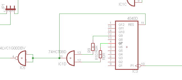
A part of design drawing

I used a 4040 counter to count the pulses from an encoder. I then connected two counter output signals to an AND gate, and after that one way is go to reset 4040 counter. The issue is that when I connect the gates in this way, there is no logic-high output signal from the 2 pins of the counter. If I disconnect them like the image below, I can read the output signal again from a multimeter, and other pins always have a signal.

I measured the AND gate and NAND gate; there are no short circuits. Why there is no output signal when connect these gate?
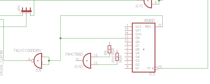
the one after i changed

\$\endgroup\$
8
  • \$\begingroup\$ I have reviewed 4040 datasheet. I have reviewed your schematic. It looks fine; the counter will increment until Q7 and Q9 are both high, then the master reset will be raised momentarily and this will reset the counter and force Q7 and Q9 low. I ask for more information: what were IC1D pins 13 and 12 connected to when R9 and R10 were removed? Can you edit the question to clearly show the two test configurations, and where you made measurements? That part of the question is confusing. \$\endgroup\$ Commented Jun 20, 2014 at 9:22
  • \$\begingroup\$ According to NXP's 4040 datasheet, Q7 and Q9 are on pins 13 and 14, respectively. It is different on your circuit diagram. (But doesn't explain the problem you observe). \$\endgroup\$
    – user36113
    Commented Jun 20, 2014 at 9:29
  • \$\begingroup\$ @JamesCameron Thank you for your reply, i disconnect IC1D totally,that means i only use Q9 goes to IC5 directly(although the counting number will become lower,but not so big difference),and i measured at Pin 12(Q9)(see the second one),but still has that problem. \$\endgroup\$
    – Mark0923
    Commented Jun 20, 2014 at 9:35
  • \$\begingroup\$ @fmunkert, yes, I noticed, the datasheet numbers from Q0, but the schematic here numbers from Q1. Mark0923, you say that with Q9 tied to master reset alone you have a problem, but I'm not sure what the problem is. You should see low output on Q9 all the time, and you would need oscilloscope or other instrument to see very brief high output on Q9. Q8 will show a signal. Q10 will not. \$\endgroup\$ Commented Jun 20, 2014 at 9:39
  • \$\begingroup\$ @JamesCameron yes, the problem is like, no matter which output i use from Texas Instruments 4040 counter, once i connect to the logic gate, it will have no out put signal, but if i disconnect that, all the signal will come back again...this is why i feel confused. my colleague said maybe because of the logic gate has a too high impedance,is it possible? \$\endgroup\$
    – Mark0923
    Commented Jun 20, 2014 at 9:52

3 Answers 3

6
\$\begingroup\$

I think you do have an output signal but it only lasts for maybe 10 nano seconds before the reset in the chip has activated and cleared everything down again. Try using a scope with a trigger function and a fast time base.

\$\endgroup\$
5
  • \$\begingroup\$ +1 In fact the pulse may be so short that it can't reliably do whatever else it is supposed to do. RC or flip-flop delay could fix it. \$\endgroup\$ Commented Jun 20, 2014 at 12:13
  • \$\begingroup\$ Agreed, I would either set a flip-flop with it, and have the next clock or Q1 clear the flip-flop ... or insert an extra couple of NAND gates between the output of the first AND gate and the master reset, as some propagation delay. \$\endgroup\$ Commented Jun 20, 2014 at 12:58
  • \$\begingroup\$ thanks a lot, according to what @andy aka said,that could be a reason, i am considering to use a RC to delay the reset signal, then i will see if it works or not. \$\endgroup\$
    – Mark0923
    Commented Jun 20, 2014 at 13:27
  • \$\begingroup\$ Or just get a divider with a synchronous reset but then your decode will need to change from N to N-1. Prob best to use a Schmitt after the RC delay to prevent double reset but it's probably not a big deal in retrospect. \$\endgroup\$
    – Andy aka
    Commented Jun 20, 2014 at 13:35
  • \$\begingroup\$ maybe use RC with Schmitt can be better, because it also needs to be considered about PCB space.i will try this one first. \$\endgroup\$
    – Mark0923
    Commented Jun 20, 2014 at 13:43
0
\$\begingroup\$

Your circuit, from a logic point of view, ought to work. Barely.

The most obvious suggestion is this: are all the unused inputs to the 74HCT08 tied to ground? And do you have a 0.1 uF ceramic capacitor connecting the 74HCT08 power to ground, connected right at the pins (or at least within less than an inch)? If the answer to either is no, I suspect that your 08 output has spikes on it that are keeping the 4040 reset. A similar capacitor on your 4040 power is also are REALLY good idea. So is a solid ground set of ground connections.

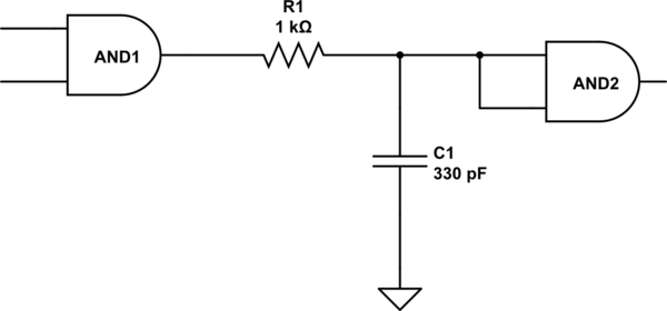
In principle, you do not need your resistors. Get rid of them. If you do want a little insurance on the pulse width of your reset pulse, try this.

schematic

simulate this circuit – Schematic created using CircuitLab

And, as with the decoupling capacitor, keep the components as close to the IC as you can.

\$\endgroup\$
1
  • \$\begingroup\$ The 74HCT08 is a quadruple AND Gate, all of 4 gates are occupied, and the 74LVC1 NAND Gate are same,so there are no unused inputs.i will try to test about your suggestions.can be not sure, that if the pulse can arrive to peak value to change the state of AND or NAND gate.seems that now the problem is the reset signal comes too fast, under this speed, the out put signal is only 20μs and only can arrive to 2V(normally it should be 4.9V),so it is not enough to change logic gate state. \$\endgroup\$
    – Mark0923
    Commented Jun 23, 2014 at 8:06
0
\$\begingroup\$

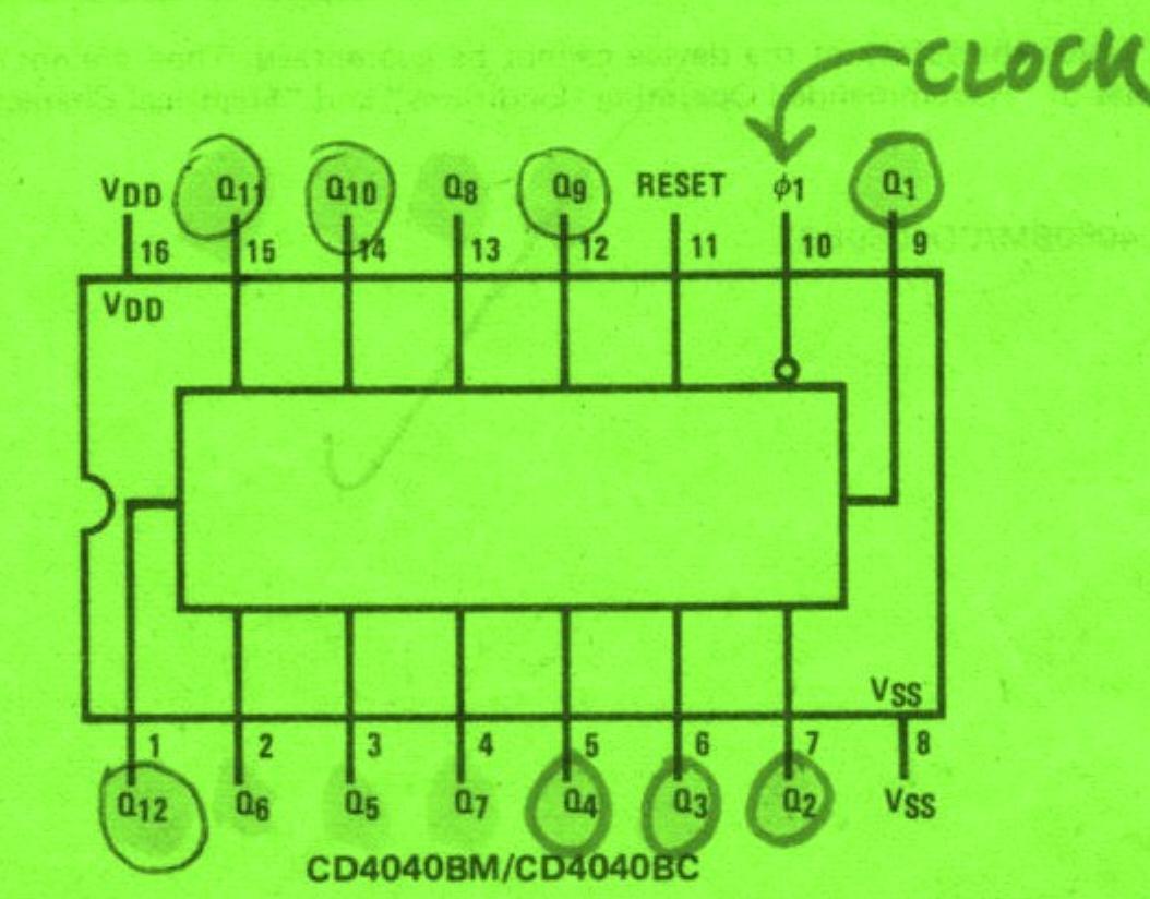
I have been having problems of a similar nature using a CD4040 being fed ok with a 2Hz clock from a CD4060 set up with a 32,768 Hz xtal. The CD4060 provides a Q14 output. I was trying to get the CD4040 to divide by 120 in order to get a one minute pulse. So I diode ANDED Q4 thru Q7 for all ones with a 22k pullup and fed the ANDED signal to the reset. Q7 NEVER WENT HIGH. I took out this circuit and strapped the reset to ground. Note that on ALL the diagrams I have, Q7 appears on pin 4. So I expected to see, and measured the signal periods on all Qs up to Q7. Q7 was now toggling OK. All was well up to Q6 which showed 32 second period. BUT Q7 on pin 4 measured 128 seconds! I then guessed that probably the circuit diagram data was wrong. And reading your report above today stating NXP data shows Q7 at pin 13, confirms that SOME DATA SHEETS HAVE AT LEAST Q7 WITH THE INCORRECT PIN NUMBER. As stated I believe Q1 to Q6 are OK. I will now search for this NXP data sheet to confirm.I will retest my circuit using pin 13.

UPDATE

I have checked my old National Semiconductor datasheet, and it seems they have marked Q0 as Q1, Q1 as Q2, Q2 as Q3 etc. So Q7 actually is on pin 13! I have not checked the other pins. This appears to offer some clue as to why YOUR reset circuit didn't work. enter image description here

\$\endgroup\$

Your Answer

By clicking “Post Your Answer”, you agree to our terms of service and acknowledge you have read our privacy policy.

Not the answer you're looking for? Browse other questions tagged or ask your own question.