11
\$\begingroup\$

I have a design using an LPC1788 together with a SDRAM module from ISSI (IS42S32800D). This is a 32bit interface.

I have routed this design out and had a prototype made with a PCB manufacturer that does 6 layer prototypes. The prototype PCB works fine. I then thought I would get the PCB manufactured in a small volume batch (100) from my usual PCB supplier. I gave them the stack up information that my prototype used to ensure there would be no issues.

However! I have massive problems with the production board. At first I was unable to raise any response from the SDRAM what-so ever with the same code I used in my prototype board. The previous board was working at 120Mhz so I was sure something was wrong with this new board. I then found a post where people suggested using Repeater Mode on the SDRAM data lines (I had not used this previously) and this raised a response from the SDRAM, however it is not stable. I can write to 16 or so addresses, but then with subsequent reads the data returned (at every address) is the data which I wrote last (probably due to Repeater Mode). When I disable repeater mode, the data returned is 0xFFFFFFF. I am now trying to connect at 48Mhz, the lowest configuration I have timings for.

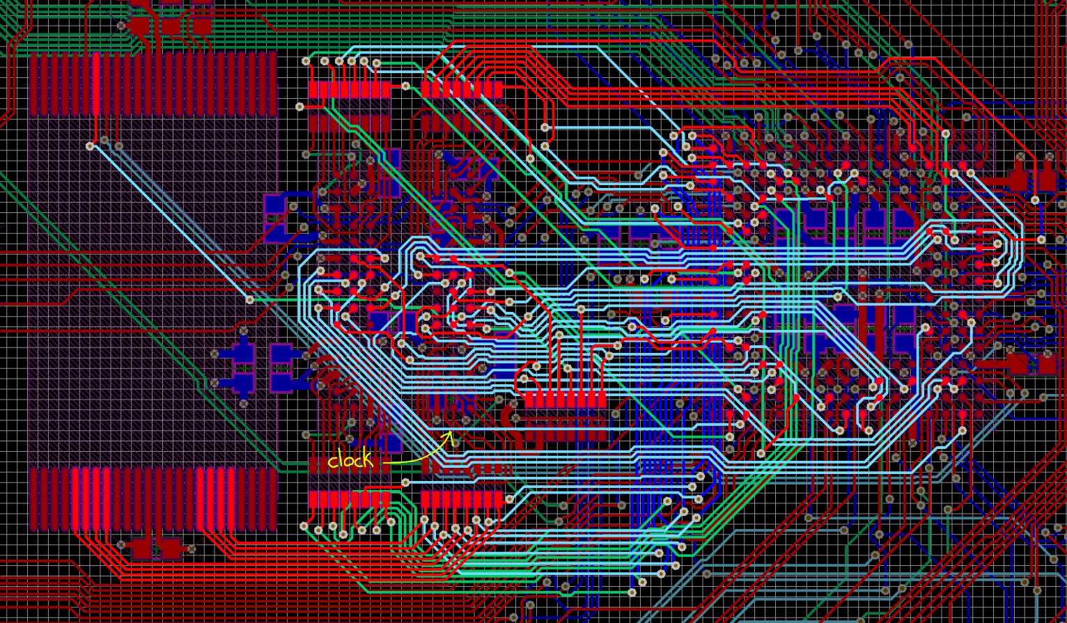
I am using the same termination resistors (on the Data lines) of 22Ohms on both boards, data lines are an average of 3cm long. Clock line is 2.4cm long. Address lines are average of 3.8cm long.

Is this too out of spec, should I delay the clock longer if it substantially shorter? I am really stuck here, as I have changed nothing about the design I was hoping for a seamless manufacture run for these boards.

Maximum Data Line Length: 59mm (Although this includes the branch to the NAND Flash)
Minimum Data Line Length (Ctrl to Res): 18mm
Maximum Address Line Length: 44mm
Minimum Address Line Length: 24mm
CLK: 24.5mm
CKE: 25mm
CAS: 28mm
RAS: 28.7mm

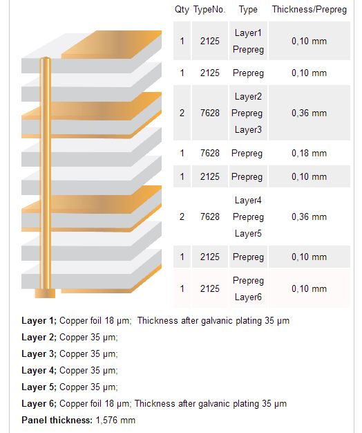
Here is the PCB stack configuration for the original (working) prototype: enter image description here
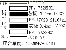
Here is the PCB stack configuration for the production (non-working) PCBs enter image description here
Here is the routing for the SDRAM: SDRAM Routing

\$\endgroup\$
12
  • 3
    \$\begingroup\$ Was the impedance control the same between proto and production runs? \$\endgroup\$
    – dext0rb
    Commented May 8, 2012 at 21:38
  • \$\begingroup\$ I am not sure. I do not know enough about signal integrity to properly define these parameters for the board houses. I felt that if if I specified parameters not knowing what I was doing I would make issues rather than fix problems. \$\endgroup\$
    – James
    Commented May 8, 2012 at 21:50
  • \$\begingroup\$ And did you pay them to verify the impedance (that @dextorb suggested you control)? \$\endgroup\$ Commented May 8, 2012 at 21:50
  • \$\begingroup\$ It's not the average length that matters. It is the minimum and maximum within the group. \$\endgroup\$ Commented May 8, 2012 at 21:51
  • 1
    \$\begingroup\$ How does the signal integrity on the clock trace look at the SDRAM pins? \$\endgroup\$ Commented May 8, 2012 at 23:55

3 Answers 3

10
+100
\$\begingroup\$

That's a lousy stackup. Your cores should be 0.2 mm and the balance of your thickness should be in the prepreg between layers 3 and 4 (Inner 1 and Inner 2).

The reason for this is that, for any signal on a trace, there needs to be a return current path on the plane right under it. The return current in the plane will try to minimize inductance (i.e. loop area), which means it will try to follow under the signal trace. If the signal trace is distant from the plane, it will look to other traces to find a return path. This is electromagnetics you're fighting.

Further, by having inner layers at different distances from their reference planes (remember, all supply rails look like grounds at AC!) compared to the outer layer distances, you create an impedance change every time you swap layers (though this can be counteracted with trace width changes, though I found it worth the trouble only once), and you significantly increase the potential for crosstalk and other interference.

Another thing you need to check is the materials used: there are over 20 different materials that call themselves "FR-4", for example. The stuff I usually use is called 370-HR. It behaves quite well with high-speed 100-500 MHz signals.

Regarding the clock line, IIRC on my last SDRAM design I had the clock set up so its edge happened last (its trace was longest by 1 cm), after all the address and data lines stabilized. So, yes, retarding the clock is worth trying. I didn't need any impedance control on the SDRAM lines.

Your termination resistors should be placed as close to the line drivers as possible. If they're not within about 0.5 cm, they can cause reflections themselves, resulting in overshoot and ringing. IMHO, 3 cm trace length is awful short to need termination resistors (I use them starting around 6-10 cm); have you tried just taking them out?

Another thing to check are your planes: Do you have signal traces crossing plane cuts? This is a huge no-no, because it forces the return current to take a long route around the cut.

Finally, edge rate is a huge problem in these designs. A lot of chips have needlessly short rise and fall times, and reducing clock frequency has no effect on this. These fast edges are great for creating reflections. This is what your 22 ohm terminator resistors are trying to fix: they slow down the edges. Though, if you're really pushing it, a tool like Mentor Graphics' HyperLynx can be used to find the optimal termination design.

Some books I can recommend to you that cover all this and a lot more, and we swear by them at work:

These books cover EMI reduction, shielding design, PCB stackup, impedance control, power supply decoupling, and a lot more. Further, Mr. Ott teaches seminars on this topic (comes with a free copy of his book).

\$\endgroup\$
9
  • \$\begingroup\$ Henry Ott's book is a bible for me in 1980. However before I read it, I was already skilled in seeing RF leakage in a mechanical/electrical design, before EMC testing even started. Slots, and radiators, and dielectric antennae, and I/O bus cables were the best antenna for ingress and egress. \$\endgroup\$
    – D.A.S.
    Commented May 14, 2012 at 9:24
  • \$\begingroup\$ Good info here, according to the Hyperlynx simulation based on my inputted simulation data, the 22 Ohm resistors are required as otherwise the waveform on the datalines (driven at 1ns rise time) from the SDRAM are horribly distored and some reflections cross the reference voltage. \$\endgroup\$
    – James
    Commented May 14, 2012 at 12:08
  • \$\begingroup\$ Also, the stackup recommendation is good. There is a minor difference in the stackup between the prototyper and the manufacturer. I'm adding the diagrams to the Question for you to see. Also - I have been reading Signal Integrity Simplified by Eric Bogatin. Good info here but will take some time to digest and sink in enough to begin a new board layout with his recommendations. \$\endgroup\$
    – James
    Commented May 14, 2012 at 12:09
  • \$\begingroup\$ For what it's worth, OP originally had what looked like Altium pics. Altium has its own set of signal integrity tools that can use IBIS files. It can also examine crosstalk. But it needs the exact stackup info to do this. \$\endgroup\$
    – ajs410
    Commented May 14, 2012 at 15:52
  • 1
    \$\begingroup\$ So at this point, I'm most concerned about the resistors. They seem to be in the middle of the traces instead of at the drivers where they belong. In these applications, it's best to not use resistor packs, but instead use small individual resistors. If you must use resistor packs, you should take the time to do a lot better job swapping the resistors to make the layout less via-crazy. That's about all I can tell from your layout, which has no package outlines and makes half the layers hard to see. \$\endgroup\$ Commented May 15, 2012 at 13:27
4
\$\begingroup\$

At this sort of frequency I think track length type issues are unlikely to be a major issue, certainly for delay issues. As the problems started with a new PCB the very first thing to do would be to test all lines for continuity (against the datasheet, not your schematic, in case your schematic has errors), and scope every pin to check that the waveforms are at least plausible - even if your scope isn't up to checking timing details it should be fairly obvious if there are any open or shorted pins.

Doing this sort of stuff without an adequate scope is fraught with potential dangers - how do you know how much margin you have ? Even if it works, how do you know whether or not you are right on the edge, and vulnerable to field/produciton failures due to tolerances, temperature or Phase of the Moon?

\$\endgroup\$
2
\$\begingroup\$

2nd add We assumed your design was margin tested and the code was perfect in your questions. (not) I suggest you verify the following;

  1. Configure the IO to have fast slew and disable the input filters
  2. Enable the input mode on the clock
  3. Set the slew bit (9?) to increase the slew rate for the SDRAM interface pins
  4. Enable repeater mode since they are bi-directional and must not be left floating on a cmos input.
  5. Change the supply voltage to determine sensitivity to error.
  6. default reset mode for a data bus pin is FUNC=0X00, MODE=0X02, HYSTERESIS=ENABLED, INVERT=DISABLED, and SLEW=STANDARD
  7. Does your call to PINSEL_ConfigPin() with a new function value, reset the MODE to INACTIVE (no pull-down/pull-up resistor) and turn off HYSTERESIS?
  8. Are you using a for/next loops or discrete code such as;

    • LPC_IOCON->P3_0 |= 1; // D0 @ P3.0
    • LPC_IOCON->P3_1 |= 1; // D1 @ P3.1
    • LPC_IOCON->P3_2 |= 1; // D2 @ P3.2 etc.
  9. Do you assert to re-enable the WE pin, every time when needed?
  10. Do you use? *pPIN &= ~(0x00000007);//Clear function bits"

I remember debugging my 1st CMOS design from a Physics post grad student for a Seismic portable recording, switchable timer logic board. There was no firmware or uC but he never did a worst case tolerance analysis and the hardware had race conditions all over the place when a dozen more boards were built and debugged by myself. The Seismic Prof brought over the Head of Physics Dept to ask why I could not make debug the boards, then I had to advise him component variation exposed many design flaws called timing race conditions due to metastable conditions and clock edge used. He still still didn't understand, then I asked him tell me how many fingers I unfolded while I was raising my hand before it reached my waist level from low to high. Then he said , you can't do that and expect a correct answer. I said, precisely. Thats a primitive race condition. They get less obvious with more levels of complexity. U of Manitoba 1973.

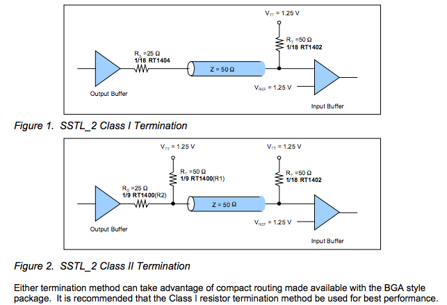
1st added: Which bus termination scheme did you use? bus method (1) is preferred, Is 1.25Vdc clean?


  1. Did pay for ICT on these boards? bare board test is a must
  2. Did you specify impedance on your gerber layout instructions?
  3. Did you run simulations on your layout with tolerances?
  4. Dielectric constant on boards and #of layers of pre-preg control the impedance of stripline and microstrip along with trace width and gap.

    There are many free online Z calculators for stripline.

    You can try to measure capacitance on large tracks or ground planes and compare both bare boards.

    Also look at the signals with a high speed scope and observe overshoot and clock<>data eye pattern.

There has to be a simple explanation for the errors, but its not easy to find. But once you find the root cause... you won't make that mistake again.

added: Another mistake I found is your stack height diagram does not indicate the Cu layer thickness and there is insufficient to fit in 6 layers unless it is wrong or the Cu thickness is 0.039 mm (NOT ;)

\$\endgroup\$
9
  • \$\begingroup\$ Just a comment for OP - I see OP is using Altium Designer, and there is an impedance calculator built into the software. I haven't used it much but I know its there somewhere! \$\endgroup\$
    – dext0rb
    Commented May 11, 2012 at 18:57
  • 2
    \$\begingroup\$ While wiring a trace (press W in PCB view), press the Tab key and you will see the estimated impedance. \$\endgroup\$
    – ajs410
    Commented May 11, 2012 at 20:31
  • \$\begingroup\$ generally for low complexity Qty 100 PWB's I would not pay for ICT (test), but these have blind tracks so I would ... something to consider... and measure the capacitance on a bare board V+<> GND \$\endgroup\$
    – D.A.S.
    Commented May 11, 2012 at 20:59
  • \$\begingroup\$ I did not pay for impedance control on these boards. The simulated lines in Hyperlynx (MentorGraphics) showed pretty much perfect (or well within spec) waveforms based on my routed design. To model this I recreated each transmission line and via along with IBIS models. I do not have a scope of sufficient bandwidth the properly investigate the actual signals =( \$\endgroup\$
    – James
    Commented May 12, 2012 at 19:18
  • 1
    \$\begingroup\$ Hello @TonyStewart, thanks for your support. 1) Prototype board did not require fast slew. Enabled with no change in effect. 2) Unsure what this means - clock is an output? 3) Hysteresis was left enabled. Disabled with no change in effect. 4) Increased slew not enabled on proto. Enabled with no change in effect. 5) Not tested. 7) Pin Config function does not alter other bits. 8) Discrete code for control pins, for loop for data/address 9) When do I need to enable WE? EMC controller should do this for me? 10) Bits are NOTed before being set. I have another prototype on order, be here next week. \$\endgroup\$
    – James
    Commented May 14, 2012 at 22:02

Your Answer

By clicking “Post Your Answer”, you agree to our terms of service and acknowledge you have read our privacy policy.

Not the answer you're looking for? Browse other questions tagged or ask your own question.