15
\$\begingroup\$

Is there an effective way to directly measure the gate capacitance of a power MOSFET, like say the IRF530N?

The way my circuit is behaving would indicate that the effective gate capacitance is perhaps double or more of the value quoted in the datasheet, which would be throwing off my op-amp stability by lowering the frequency of the op-amp \$R_O\$+\$C_{iss}\$ pole.

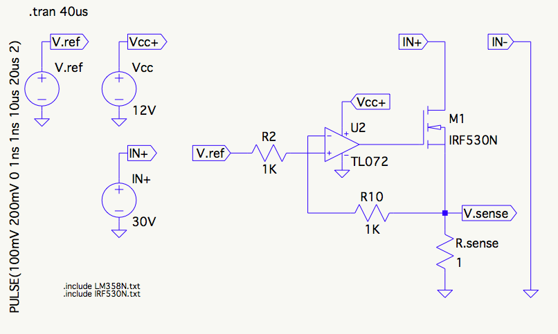
Here's the circuit schematic in case that's a help, but I'm really just interested in the general case of a test fixture I can wire up, pop an arbitrary TO-220 MOSFET in there and calculate the effective capacitance from a scope trace or something like that.

enter image description here

Is there a practical way to make a useful measurement of MOSFET input capacitance on the bench?


Outcome Report

Both the answers provided key insights. In retrospect, I think the short answer to my direct question would be: "How do I measure gate capacitance? At many different combinations of gate and drain voltages!" :)

Which represents the big insight for me: A MOSFET does not have a single capacitance. I think you need at least two charts to make a decent start at describing the ranges, and there is at least one condition where the capacitance can be way more than the quoted \$C_{iss}\$ value.

Regarding my circuit, I made some improvements by switching out the IRF530N with an IRFZ24N having less than half the quoted \$C_{iss}\$ value. But while that overcame the first instability, the following tests it enabled showed full-out oscillation at higher currents.

My conclusion is that I need to add a driver stage between the op-amp and the MOSFET, presenting a very low effective resistance to the MOSFET input capacitance and driving the pole it creates up well past the 0dB frequency of the op-amp. Not mentioned in the original post is that I require pretty decent speed, say 1µs step response, so applying heavy-handed compensation to the op-amp to achieve stability is not a viable option; it would simply sacrifice too much bandwidth.

\$\endgroup\$
2
  • \$\begingroup\$ From the datasheet, the IRF530N gate capacitance is more than 100pF. That's well within the performance of high quality capacitance meters (they can measure capacitances of just a few picofarades). You'd need to disconnect the gate and use a capacitance meter. \$\endgroup\$
    – PkP
    Commented Aug 22, 2015 at 19:28
  • \$\begingroup\$ @PkP scanny asked for the effective gate capacitance, which is much higher than what you'd measure statically. \$\endgroup\$ Commented Aug 23, 2015 at 8:17

3 Answers 3

4
\$\begingroup\$

This answer does not address how to measure FET \$C_{\text{iss}}\$, because there is no real value in doing that. Since capacitance is such an important FET parameter, the manufacturers provide capacitance data on every datasheet that is definitive in almost every situation. (If you find a datasheet that doesn't provide full data on the capacitance, then don't use that part.) Given the data in the datasheet, trying to measure gate capacitance yourself is a bit like trying to take a picture of Yosemite while Ansel Adams is there to hand you that picture he took.

What is worthwhile is understanding the characteristics of \$C_{\text{iss}}\$, what they mean, and how they are effected by circuit topology.

Facts about \$C_{\text{iss}}\$, that you already know

  • \$C_{\text{iss}}\$ = \$C_{\text{gs}}\$ + \$C_{\text{gd}}\$
  • \$C_{\text{gs}}\$ is nearly a constant value, mostly independent of operating voltages.
  • \$C_{\text{gs}}\$ is not related with and has no involvement with the Miller effect.
  • \$C_{\text{gd}}\$ is strongly inversely dependent on \$V_{\text{ds}}\$, and can easily change by an order of magnitude throughout the operating voltage range.
  • \$C_{\text{gd}}\$ is the parasitic cause of the Miller effect.

Interpretation of these seemingly simple, but subtle facts can be tricky and confusing.

Wild and Unsubstantiated Claims Regarding \$C_{\text{iss}}\$ -- For the Impatient

The effective value of \$C_{\text{iss}}\$, of how it is manifest, depends on circuit topology, or how and what the FET is connected to.

  • When the FET is connected in circuit with impedance in the source, but no impedance in the drain, meaning that the drain is connected to an essentially ideal voltage, \$C_{\text{iss}}\$ is minimized. \$C_{\text{gs}}\$ will virtually disappear, its value being divided by FET transconductance \$g_{\text{fs}}\$. This leaves \$C_{\text{gd}}\$ to dominate the apparent value of \$C_{\text{iss}}\$. Are you skeptical of this claim? Good, but don't worry it will be shown to be true later.

  • When the FET is connected in circuit with impedance in the drain, and zero impedance in the source, \$C_{\text{iss}}\$ is maximized. Full value of \$C_{\text{gs}}\$ will be apparent, plus \$C_{\text{gd}}\$ will be multiplied by \$g_{\text{fs}}\$ (and drain impedance). Thus \$C_{\text{gd}}\$ will dominate \$C_{\text{iss}}\$ (again), but this time, depending on the nature of the impedance in the drain circuit, could be unbelievably massive. Hello Miller plateau!

Of course, the second claim describes the most common use case for hard switched FETs, and is what Dave Tweed talks about in his answer. It is such a common use case that manufacturers universally publish Gate Charge charts of it, along with circuits used to test and evaluate it. It ends up being the worst possible maximum case for \$C_{\text{iss}}\$.

The good news here for you is that if you have accurately drawn your schematic, you don't have to worry about the Miller plateau, because you have the case of the first claim with minimal \$C_{\text{iss}}\$.

Some Quantitative Details

Let's derive an equation of \$C_{\text{iss}}\$ for a FET connected as in your circuit. Using a small signal AC model for a MOSFET such as Sze's 6 element model:
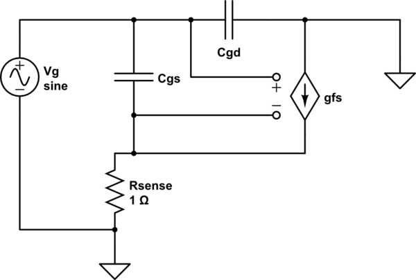
schematic

simulate this circuit – Schematic created using CircuitLab

Here I've discarded the elements for \$C_{\text{ds}}\$, \$C_{\text{bs}}\$ (bulk capacitance), and \$R_{\text{ds}}\$ (drain to source leakage), because they're not needed here and just complicate things. Find for \$Z_g\$:

\$\frac{V_g}{I_g}\$ = \$\frac{g_{\text{fs}} R_{\text{sense}}+1}{s \left(C_{\text{gd}} \left(g_{\text{fs}} R_{\text{sense}}+1\right)+C_{\text{gs}}\right)}\$ \$\frac{\frac{s C_{\text{gs}} R_{\text{sense}}}{g_{\text{fs}} R_{\text{sense}}+1}+1}{\frac{\text{Cgs} s C_{\text{gd}} R_{\text{sense}}}{C_{\text{gd}} \left(g_{\text{fs}} R_{\text{sense}}+1\right)+C_{\text{gs}}}+1}\$

Now, the second fractional term doesn't do anything until frequency is well above 100 MHz, so we'll just treat it as unity. That will leave the first fractional term, the integrator term, which is the capacitive impedance. Then rearrange to get the effective \$C_{\text{iss}}\$ that matches the topology:

\$C_{\text{iss_eff}}\$ = \$\frac{C_{\text{gd}} \left(g_{\text{fs}} R_{\text{sense}}+1\right)+C_{\text{gs}}}{g_{\text{fs}} R_{\text{sense}}+1}\$ or \$\frac{C_{\text{gs}}}{g_{\text{fs}} R_{\text{sense}}+1}+C_{\text{gd}}\$

Note that here \$C_{\text{gs}}\$ is divided by \$g{\text{fs}}\$ (and \$R_{\text{sense}}\$) , hence obscured by transconductance, and \$C_{\text{gd}}\$ is added unmodified. Also, if \$R_{\text{sense}}\$ = 0, \$C_{\text{iss}}\$ = \$C_{\text{gs}}\$ +\$C_{\text{gd}}\$.

For an IRF530N at \$V_{\text{ds}}\$ = 25V, \$C_{\text{gs}}\$ = 900pF, \$C_{\text{gd}}\$ = 20pF, \$g_{\text{fs}}\$ = 20S: \$C_{\text{iss_eff}}\$ = 63pF. LM358 with 63pF loading ends up with about \$35^{\circ }\$ phase margin ... not oscillatory, but pretty ringy.

But, if \$V_{\text{ds}}\$ where to fall to 3V, \$C_{\text{gd}}\$ would increase to ~200pF (Fig 5 in datasheet), and \$C_{\text{iss_eff}}\$ increase to 243pF. And when using a LM358 OpAmp, with open loop output impedance of ~2kOhms at the crossover frequency, that turns out to be a problem.

Let's look at the response. I'll use a Nichols chart here because that will show open loop and closed loop response simultaneously.
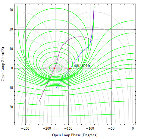
enter image description here

Here, the rectilinear grid is the open loop, while the contour lines show the closed loop (green contours for dB magnitude and gray contours for phase). The blue curve is \$V_{\text{ds}}\$ of 25V, and at the crossover point (at the red dot -- 502kHz), phase margin is indeed \$35^{\circ }\$, and closed loop peaking of about 5dB.

The purple curve is for \$V_{\text{ds}}\$ of 3V, and the corresponding open loop phase margin is ~ \$-3^{\circ }\$. For the closed loop, look at the ascent of mount Nichols, the curve pretty much nails the peak which would ideally correspond to infinite peaking. Of course that won't happen, but the system would be unstable.

It is no surprise that the main problem here is the open loop output impedance of the LM358. Even with a FET-circuit topology that has minimal expression of \$C_{\text{iss_eff}}\$, the LM358 is not adequate. An amplifier with open loop impedance of 50 Ohms or less and phase margin greater than \$75^{\circ }\$ would probably solve the stability problems.

\$\endgroup\$
3
  • \$\begingroup\$ Awesome answer @gsills! How did you produce that Nichols chart? Makes me want to study that alternative to my usual Bode plots :) I totally ended up at the same conclusion, my original question was wrong-headed; but often those are the ones one learns most from, as was certainly the case here :) \$\endgroup\$
    – scanny
    Commented Aug 28, 2015 at 21:46
  • \$\begingroup\$ Thanks @scanny. I've written a Mathematica package to create Nichols, Bode, and a couple of other types. Bode plots are the work horse, but I don't know why Nichols charts aren't used more. This has been a great series of questions. The circuit appears much simpler than it is. \$\endgroup\$
    – user16497
    Commented Aug 29, 2015 at 2:07
  • \$\begingroup\$ @gsills: Please clarify this: Now, the second fractional term doesn't do anything until frequency is well above 100 MHz, so we'll just treat it as unity. \$\endgroup\$
    – emnha
    Commented Sep 10, 2017 at 17:56
13
\$\begingroup\$

The gate capacitance of a MOSFET is a more complicated topic than a lot of people realize. It depends very strongly on the operating conditions of the device. This makes sense — the capacitance we're talking about has the gate itself as one plate, which is a fixed physical structure, but the other "plate" is not just the source, drain and substrate structures nearby, but also the charge carriers flowing in the source-to-drain channel, and their concentration varies considerably.

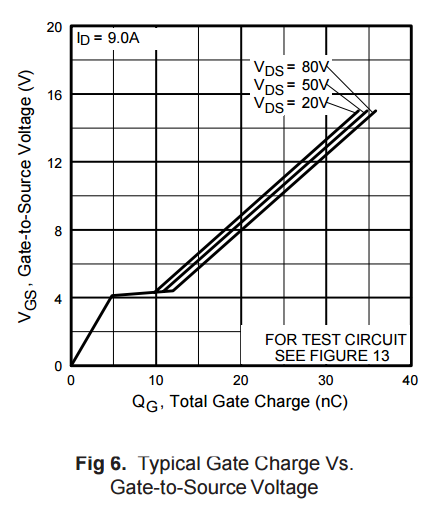
To get some insight into this, look at Figure 6 in the IRF530N datasheet (reproduced below), which shows the gate charge as a function of gate-source voltage. The definition of capacitance is \$\frac{\Delta charge}{\Delta voltage}\$, so given how this chart is laid out, the effective gate capacitance is the inverse of the slope of the curve at any given point.

IRF530N Figure 6

The \$C_{ISS}\$ value is measured at \$V_{GS}\$ = 0V, so it corresponds to the slope at the lower-left corner of the graph. But note how the graph flattens out near the threshold voltage — this reduced slope indicates a much greater effective capacitance (roughly 10×) at that operating point. And more to the point, this is exactly the point at which your current regulator circuit is operating.

So, to fully characterize the load capacitance your opamp is seeing, you need to test the MOSFET in the manner shown in Figure 13, with suitable bias voltages on the gate and drain.

\$\endgroup\$
2
  • \$\begingroup\$ This is very interesting indeed Dave. I think I'm coming up against this very "10x threshold capacitance" (or whatever it would be called) that you mention. I was able to largely overcome the \$V_{DS}\$ stability dependence I identified with the help of Spehro's answer, by substituting a lower capacitance MOSFET. But now I'm getting a 500kHz oscillation right around 4.35V \$V_{GS}\$ (\$I_{DS}\$ = 400mA) and continuing until \$I_{DS}\$ gets to about 2.4A, at which point it very abruptly disappears. This is certainly consistent with this chart. I think it's time to add a driver stage :) \$\endgroup\$
    – scanny
    Commented Aug 24, 2015 at 3:43
  • 2
    \$\begingroup\$ After further research, I've learned that the "10x threshold" part of the graph is known as the Miller plateau. Also I learned that my circuit won't reach that level, because that breakpoint indicates where the drain voltage begins to drop because the current compliance of the source behind it is exhausted. Since I'm staying in the linear region where the source voltage remains constant, it seems I'm at least safe from that big bump in incremental capacitance :) \$\endgroup\$
    – scanny
    Commented Aug 26, 2015 at 6:46
7
\$\begingroup\$

You can ground the source, connect the drain to the desired bias voltage (with a large capacitor - maybe 1uF ceramic) across drain-source) and directly measure the gate capacitance with a battery-powered meter or LCR bridge. The Vishay datasheet says around 0.7nF at 30V and 1nF at 2V Vds (for Ciss).

If you don' t have a C meter, a reasonably small value (maybe 0.5 volt) square wave can be applied to the gate through a suitable resistor (maybe 1K) and you can observe the charge/discharge times to 1/e with a scope (x10 probe), then subtract the scope probe capacitance.

\$\endgroup\$
3
  • 2
    \$\begingroup\$ Very useful answer @Spehro! :) When you mentioned the two values at different \$V_{DS}\$, it caused me to revisit the datasheet and I realized \$C_{iss}\$ was not single-valued. In returning to my circuit on the bench, I see I can vary the step response from 1-bump to like 10 bumps, just short of oscillation, simply by changing the \$V_{DS}\$ from 30V to 1V! Even better, I can duplicate those results on the simulation! :) This is a critical insight for me on this little project. I had been using various voltages without seeing the relationship and wondering why my results seemed random :) \$\endgroup\$
    – scanny
    Commented Aug 23, 2015 at 1:28
  • 1
    \$\begingroup\$ Separate topic; What's the purpose of the 1uF capacitor between drain and source on the test fixture? \$\endgroup\$
    – scanny
    Commented Aug 23, 2015 at 1:34
  • 2
    \$\begingroup\$ @scanny we want a bias voltage with drain and source shorted for AC signals. If the test setup ran long leads to a power supply there would be some inductance in series which might screw up the reading. Not so likely with a high capacitance MOSFET as the OP has, but it's supposed to be a general test jig. \$\endgroup\$ Commented Aug 23, 2015 at 13:02

Your Answer

By clicking “Post Your Answer”, you agree to our terms of service and acknowledge you have read our privacy policy.

Not the answer you're looking for? Browse other questions tagged or ask your own question.