16
\$\begingroup\$

I've been working with fpgas for years, and always used synchronous resets for every parts (that need it) of my circuits. It helps the circuit to be globally reset at a given clock cycle.

However, I was told that in ASIC circuits, people tend to use asynchronous reset everywhere. I'm wondering why, and if it is the case in some fpga designs too. I would love to hear professional opinions.

Thanks

\$\endgroup\$

5 Answers 5

12
\$\begingroup\$

There seem to be a lot of views on this one.
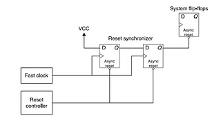
Asynchronous assertion, synchronous deassertion is said to be good practice. This avoids the issue of the clock not running (or running too slowly to capture the reset signal) on synchronous assertion, and possible metastability on asynchronous deassertion.

You would use a reset synchroniser (two FFs) with the output tied to the rest of the designs resets:

Reset

Couple of discussions:
Async and sync reset
Letters On Sync vs. Async Resets

\$\endgroup\$
6
  • \$\begingroup\$ How do the setup/hold time requirements between the release of a latch's reset signal and its clock compare with those for the data input? I would feel more comfortable if the latches in the system saw the end of the reset signal occur on the inactive clock edge. Would the release of an async reset on an active clock edge be guaranteed not to affect the cycle where it occurs? \$\endgroup\$
    – supercat
    Commented Nov 2, 2011 at 16:06
  • \$\begingroup\$ No, the release of reset asynchronously is not guaranteed to be clean due to reset recovery time needed (like setup/hold) This is why you would release the reset synchronously. \$\endgroup\$
    – Oli Glaser
    Commented Nov 2, 2011 at 17:07
  • \$\begingroup\$ My question is whether having a latch1 release the reset signal feeding latch2 on the same clock edge as latch2 would be using is completely kosher, i.e. whether the minimum propagation time from latch1's clock to its output would satisfy hold requirement for latch2's reset input. BTW, what do you think of my answer above? The circuit you drew offers little immunity to runt pulses on the reset line, when almost total immunity should be possible. \$\endgroup\$
    – supercat
    Commented Nov 2, 2011 at 23:18
  • \$\begingroup\$ Upon further consideration, one could add protection from runt pulses by adding a third latch, and having its async reset signal be a glitch-suppressed version of the signal fed to the first two, such that a signal which asynchronously disturbed the third latch would be guaranteed to cleanly reset the first two. A runt pulse on the reset input could cause the main reset line in the chip to get a runt pulse, but if such a pulse occurred it would be followed by a synchronous reset pulse. \$\endgroup\$
    – supercat
    Commented Nov 2, 2011 at 23:37
  • \$\begingroup\$ Sorry, I think I see what you mean now. If you mean the output from the second latch in the synchroniser to system FF reset, my understanding is that the reset recovery time is typically less than the data setup time for the same FF, so it should be okay. I agree about the runt pulses, it offers no immunity to those without something like you suggest being implemented. \$\endgroup\$
    – Oli Glaser
    Commented Nov 3, 2011 at 0:25
7
\$\begingroup\$

I would favor an asynchronous reset over a synchronous reset for a few reasons (in no particular order):

  • Adding an asynchronous set or reset function to a flip-flop will probably result in a smaller design due to the integration of the logic into a single cell (vs. a non-resettable flip-flop with an AND gate on the input)
  • Fewer gates results in less congested wiring / place and route
  • It is a simpler/easier process to reset the chip (more user/test friendly)
  • Making the reset path asynchronous simplifies the static timing analysis partitioning of the reset signal
  • A synchronous reset would add extra logic into the data flow critical path, and make it more difficult to meet setup and hold requirements
  • While a FPGA has a 4-6 input arbitrary logic function on the input, you "pay" for each input into a gate on an ASIC (more inputs = larger gate; complex functions = multiple gates)

Ultimately I don't think any of these issues are show-stoppers, but they would definitely contribute to a strong preference of asynchronous reset on ASICs.

\$\endgroup\$
1
  • 3
    \$\begingroup\$ One danger with using bringing asynchronous resets into one's internal logic is that a runt pulse on the reset input may wreak any and all manner of havoc. If one is going to allow one's circuitry to be reset asynchronously, one should design the input circuitry in such a way as to ensure that any reset pulse sufficient to possibly cause any type of asynchronous reset to reach the internal circuitry will be guaranteed to also cause a synchronous reset to occur. \$\endgroup\$
    – supercat
    Commented Nov 3, 2011 at 19:36
5
\$\begingroup\$

Asynchronous reset with synchronous de-assertion works very well. As mentioned above, async reset flops are smaller and don't require a clock active to ensure reset, so you can force a part into reset (usually a known, low power state) with just power and a single hard wired pin or power-on reset.

If you really want to dig into this, you might read over Cumming's papers on this, in particular:

http://www.sunburst-design.com/papers/CummingsSNUG2003Boston_Resets.pdf

Cheers.

\$\endgroup\$
6
  • \$\begingroup\$ One issue I think Mr. Cummings misses in his paper is that while glitch detectors may suppress what would otherwise be runt pulses, they can also turn what would be legitimate-length pulses into runt pulses. The effect of this is that a pulse which is just the right length could arbitrarily clobber the system state without causing a proper reset. Since it's very difficult to avoid metastability in all cases without double-synchronization, I would suggest having two async-capture circuits, one of which has a 'stricter' glitch-detect criterion, and then... \$\endgroup\$
    – supercat
    Commented Nov 3, 2011 at 22:27
  • \$\begingroup\$ ...arrange things so that a short glitch may or may not cause a reset to occur one or two cycles later, but a long enough pulse will cause an immediate reset. Also, while using 'async reset' inputs on flip flops may aid synthesis in some topologies, that doesn't mean they must be used asynchronously. It may be helpful to have most internal reset signals be synchronized to the clock even when driving "async reset" inputs on latches. \$\endgroup\$
    – supercat
    Commented Nov 3, 2011 at 22:34
  • \$\begingroup\$ Cummings does say glitch filters "are ugly." I've never seen one in the ICs I've worked on. We tend to use Schmitt-triggers at all input pad cells to avoid these problems, and the power-on resets I use are similarly cleaned up. By the way, in what cases would you have short pulses on a reset line? I've seen this in some scan test scenarios, but they are still on the order of as clock cycle long, not purposeful short pulses. On your last comment, the deassertion of reset must be synchronized to the clock to avoid s/h violations on the reset, and ensure all flops exit reset on the same edge. \$\endgroup\$ Commented Nov 4, 2011 at 0:13
  • \$\begingroup\$ Glitch filters are often useful for determining which types of inputs can cause metastability, but they don't eliminate metastable states. The goal with a glitch filter should be to ensure that any metastable states which may occur are in "don't-care" situations. Sometimes it's necessary to have one device be capable of resetting another device which is plugged into it. Unless the reset wire is double-synchronized, there will be a risk of runt pulses from nearby ESD events and other such nasties. \$\endgroup\$
    – supercat
    Commented Nov 4, 2011 at 14:58
  • \$\begingroup\$ As for the last point, I was merely saying that even one is synthesizing a design on hardware that provides "free" async reset inputs on flip flops, that doesn't mean one can't fully synchronize the signal to the main clock on both assertion and release. Outward-facing signals may have to react asynchronously to a reset input, but that doesn't mean one needs to asynchronously reset all one's latches. Indeed, to avoid inconsistent states, it may be useful to just have all but two of the latches in one's design be synchronous. \$\endgroup\$
    – supercat
    Commented Nov 4, 2011 at 15:06
2
\$\begingroup\$

Another approach, which would seem even safer than the 'async assert/sync release' approach, would be to have an asynchronous reset detector (much as described elsewhere, with asynchronous 'assert' and synchronous 'release'), but have the output from that gate any outward-facing I/O devices without asynchronously resetting anything (other than the latch in the detector itself). If one uses two asynchronous reset detectors, one for I/O lines and one to feed the synchronous reset detector, and if one designs the one for I/O lines so that it will only be tripped by reset pulses which are sound enough to reliably trip the main detector, one may avoid even having the outputs glitch in cases that aren't going to reset the CPU. Note that if one does this, a legitimate-length reset pulse will reset the outputs asynchronously, but a runt reset pulse may not cleanly reset the outputs until two clock cycles later (if the runt reset pulse is followed by a real one before two clocks have arrived, the real reset pulse will reset the outputs even if the runt pulse didn't).

Another thing to consider is that systems often have some registers which are not supposed to be affected by a reset. If an asynchronous reset could hit circuitry which writes to those registers, it would be possible for a reset pulse which arrives at the wrong time to clobber those registers, even if it's a clean (non-runt) pulse. For example, if code is trying to write to address 1111 and an async reset which arrives just before a clock pulse forces one of the address latches to zero just as the clock pulse is arriving, that could cause an erroneous write to address 1110. While one could use multiple internal reset lines with combinatorial delays to ensure that register writes were disabled before the address got clobbered, using synchronous internal reset logic avoids the issue altogether.

BTW, here's a circuit illustrating the concept. Near the lower-left corner are two logic inputs for reset. One will generate a "clean" reset pulse, and the other will generate a really icky one. The yellow LED indicates main system reset; the cyan LED indicates I/O enable. Hitting a clean reset will cause an immediate "reset" of the outputs; hitting an icky reset will either cause a delayed reset of the outputs, or leave them unaffected (in the simulator, there's no way to cause the 'leave them unaffected' case).

\$\endgroup\$
1
  • \$\begingroup\$ I think this sounds like a good idea. so many shades of grey with seemingly simple things like reset. \$\endgroup\$
    – Oli Glaser
    Commented Nov 3, 2011 at 0:28
-1
\$\begingroup\$

As an experienced engineer (3 years with FPGA design and embedded systems), I'm telling you that you need to check the FPGA's datasheet and user guide. Its not a simple answer.

You have to make your design FITs the FPGA type you chose. Some FPGAs have FlipFlops that were designed for Async reset, some are designed for Sync reset.

You have to check the FPGA user guide for what type of FlipFlops you have.

The Implementor/Mapper will chose dedicated routes for your reset (code can run at higher freq and takes less space) if you match your code with the FPGA primitives type.

Your design will work in ANY case, but sometimes the FPGA Implementor will go out of its way to make your logic work (adds more logic), but that will cause lower maximum frequency and/or more FPGA ressources.

Example: tested with Xilinx's ZYNQ (FPGA is designed for synched reset - see primitives user guide). By changing reset from async to sync, max stable frequency went from 220MHz to 258MHz and so I passed my frequency margin.

Also I might add that the Implementor does not know what is a clock and reset signal. It assigns flipflop pins to signals by ORDER, not by name. So in some FPGAs, the implementor choses the first signal after "process() begin" in VHDL as the clock, in some as the reset, depending on what FPGA the implementor is set to.

\$\endgroup\$
1
  • \$\begingroup\$ I disagree with your statement that "the Implementor does not know what is a clock and reset signal". The synthesis tools infer which is clock and which is reset by how they are used. The clock signal is used with an edge specification, the reset is not. Furthermore, any flip-flop can be used with a synchronous reset specification and, as you observed, this often leads to faster critical paths. \$\endgroup\$
    – Joe Hass
    Commented Feb 3, 2014 at 21:28

Your Answer

By clicking “Post Your Answer”, you agree to our terms of service and acknowledge you have read our privacy policy.

Not the answer you're looking for? Browse other questions tagged or ask your own question.