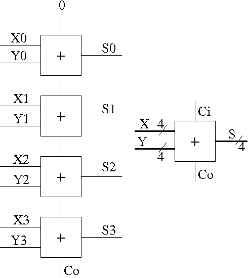
So I am learning digital logic and have learned how to create an adder and have come across this question. So I am creating a 4 bit adder. To create the 4 bit adder I just make one 1 bit full adder and stack four of them together and flow the carry out into the carry in of the next adder. The two numbers (a and b) are represented into individual 4 bit segments, one bit for each adder. So a0 b0 a1 b1 etc...
Whenever creating the full adder into an ic and seeing images online, there are multiple data bit widths. So the chip says 4 bit adder and the two inputs have a slash through them and say 4. How would you physically implement this? Is this a symbolic notation so instead of having to say a0 b0 etc... everytime, you would just use the slash symbol with the number of bits? Bits are electrical pulses. The presence of electricity and the absence of electricity represented by 1s and 0s. So how can you implement 4 bits over one line? Is it somehow controlled by the clock? Can someone please help me any ideas?

