0
\$\begingroup\$

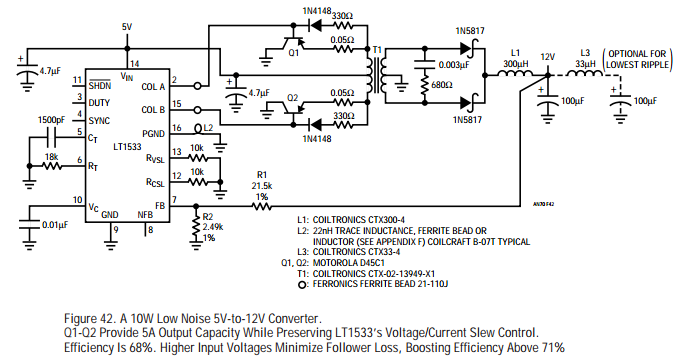
I was reading through Linear Technology's AN70 application note and on Figure 42 there are two parts of the circuitry that I can't understand.

  1. It looks like an emitter follower but there is a resistor in series of Q1 emitter. Why is it needed? And if it is needed why not in the base path of Q1?
  2. There is a series RC in parallel with the the transformer before the rectifiers at the output stage of the transformer. Is it some kind of filtering?

Can anyone explain how exactly it works?

AN70 Figure 42

\$\endgroup\$
1
  • 2
    \$\begingroup\$ I would say current limiting for the 0.05 ohm and a snubber circuit to reduce switching spikes. \$\endgroup\$ Commented Mar 7, 2017 at 11:27

1 Answer 1

2
\$\begingroup\$

The Q1 and Q2 circuits act as current amplifiers. Col A/B pins drive through a current sensing resistor on-board the chip to power ground. The addition of the emitter resistor couples the "load" current back to the base and thereby back to the sensing resistor. Without it, the current sensing part would not function.

The RC after the amplifier are to dampen the higher frequency components of the switching.

\$\endgroup\$

Your Answer

By clicking “Post Your Answer”, you agree to our terms of service and acknowledge you have read our privacy policy.

Not the answer you're looking for? Browse other questions tagged or ask your own question.