4
\$\begingroup\$

I am designing two stage operational amplifier in CMOS technology. After sizing all transistors and preeliminary checks I wanted to determine input offset voltage of my circuit, and browsing many pages with simillar questions, I actually did not find answer that would make thing clear for me.

First of all, most of the answers in that topic assume that by applying only common voltage to both inputs the Op-Amp output would be 0, which is basically not truth, as there will always be some Common Output Voltage. And this Common Output Voltage is already affected by Input Offset Voltage.

And here is where I am unable to handle this problem. I think applying any resistor divider etc could not work as any obtained result will be useless without knowledge about common output voltage. That seems as a vicious circle to me.

Should I just make spice .op to make input pair's VGS to be equal, or there's a better way to simulate the offset value?

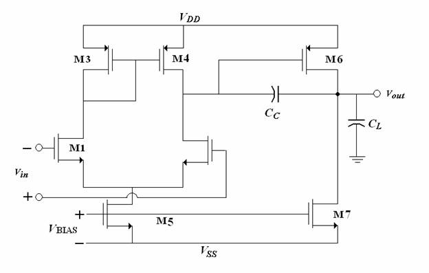
enter image description here

\$\endgroup\$
9
  • \$\begingroup\$ If you have any imbalance in operating conditions in the differential paths, such as one device being current-mirror and its "mate" being used as FET diode, the Voffset will be huge. Note the M3 to M4 imbalance. \$\endgroup\$ Commented Feb 18, 2018 at 2:18
  • \$\begingroup\$ Without a suitable feedback loop, it will be unstable and tend to latch high or low at the output. \$\endgroup\$
    – user105652
    Commented Feb 18, 2018 at 2:25
  • \$\begingroup\$ Sparky256 please forgive that missaprehension, I have added an image of my two stage opamp configuration. analogsystemsrf, I understand that having single-ended configuration I will always have mismatch, but still deciding on that configuration I would like to be able to find the offset.. \$\endgroup\$
    – Nedvved
    Commented Feb 18, 2018 at 2:27
  • \$\begingroup\$ Put a common mode voltage and a differential voltage on Vin and .step the differential voltage to find where Vout=0. \$\endgroup\$
    – τεκ
    Commented Feb 18, 2018 at 2:28
  • \$\begingroup\$ Your output stage is class A, so it will have little drive current. That is outside of any offset issues. \$\endgroup\$
    – user105652
    Commented Feb 18, 2018 at 2:29

4 Answers 4

2
\$\begingroup\$

When dealing with real world op-amps there are two major offset parameters: input offset error and output offset error. Generally, these are combined into one parameter because they are difficult or impossible to separate in practice. So, you will rarely read about output offset error, even though it is a real metric of the design. Instead, output offset and input offset errors are combined into one characteristic, and it is called "input offset error".

How to measure input offset error? (i.e. The total of input & output offset errors as explained above.) The easiest, most practical way is to configure the op-amp as a unity gain buffer ( connect output to the minus input). Apply a voltage, within the common mode range of the op-amp, to the positive (i.e. non-inverting) input. The difference between the applied test voltage and the output voltage is virtually totally attributable to the input offset error of the amplifier.

You can connect a DVM set to its lowest range between the output and the NI input and read the actual input offset voltage value directly, assuming you have a sensitive enough DVM. Vary the test voltage across the common mode input range to find the worst case.

I'm not a SPICE guy, but I'd expect you can do the same thing in a SPICE model.

\$\endgroup\$
10
  • \$\begingroup\$ The OP does not have a good design to begin with. M5 and M7 cannot have the same bias voltage. M7 makes the output class A with little drive current. The middle-section high-gain stage is missing. A Spice model of this is likely to be a mess. \$\endgroup\$
    – user105652
    Commented Feb 18, 2018 at 5:14
  • \$\begingroup\$ Sparky: You are very probably correct. I am not a discrete transistor designer, but I know op-amps very well. I am simply answering the OP's question, which seems to me to be in essence: How do you measure input offset voltage of an op-amp. \$\endgroup\$
    – FiddyOhm
    Commented Feb 18, 2018 at 11:57
  • \$\begingroup\$ @Sparky256 This is a very typical 2-stage Miller-compensated OTA (it is not an Opamp). The only difference with a real-life implementation will be that you never use that type of Miller compensation. Versions using a Miller-capacitor are typically used as an educational example. \$\endgroup\$
    – Sven B
    Commented Feb 18, 2018 at 19:35
  • \$\begingroup\$ And having the same bias voltage does not imply equal/less current. You can increase the W/L of M7 to scale the current. \$\endgroup\$
    – Sven B
    Commented Feb 18, 2018 at 19:36
  • \$\begingroup\$ FiddyOhm, your answer gave me some hints on how it should have been done, thanks. Sparky, indeed what I was doing in the design - my M7 size is about 3x M5 W/L, which gives 3x bigger current. Generally I don't think anything is missing in my design, everything was calculated primarily according to Allen Holberg's CMOS Design book, and additionally adjusted after simulations, which led to meeting most specifications. My problem was mainly with simulation techniques. Sven B, can you tell me what is beign used instead of miller capacitance in real life implementation? \$\endgroup\$
    – Nedvved
    Commented Feb 18, 2018 at 22:26
1
\$\begingroup\$

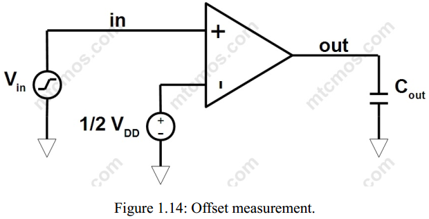
The common approach to specify the opamp's offset value is to define what should the input Vin values be when Vout is equal to VDD/2. For example, when VDD = 3.3 V, it is desired that the output is VDD/2 = 1.65 V to have full swing for the output signal. The input voltages are also often equal to VDD/2. Hence, you set Vin+ and Vin- to 1.65 V and do .dc analysis where Vin+ is swept to find its value so that Vout is equal to 1.65 V.

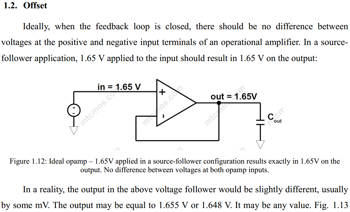
I'm surprised, as you said, you did not find the answer to that questions in books. The position I have at hand is https://payhip.com/b/5Srt and the offset issue is described in, unfortunately paid version of the book, ch. 1.2:

offset

But you should really be able to find it in other books as Razavi or Baker, see: http://www.designers-guide.org/Books/.

The voltage follower (unity gain buffer) configuration is fine to test offset voltage, but also the following testbench may be used:

offset testbench

As the last word, your design is fine. It is a classical 2-stages class A opamp. It is very often used in analog IC design. The offset value may be defined for any opamp architecture single-ended or differential. For your architecture you may consider adding zero nulling resistor (see Fig. 3.2 from https://payhip.com/b/5Srt. Click Preview button - it is in the free version) to achieve better phase margin.

\$\endgroup\$
0
\$\begingroup\$

Offsets result from scaling errors in manufacture of the MOSFETs, and manufacture variation is not a SPICE parameter. What you can do, is to use device models with some random variation in the Vth threshold voltage, and perhaps into the channel length, to mimic the expected variations. There is no simple "offset value", but rather an expected variability in the offset will give rise to a distribution of values clustering around '0'; the important variable is the width of the distribution (or, of some box that encloses the distribution and whose sidewalls are 'worst-case' specifications).

This requires some known characteristics of the manufacture be tested against your models (when the deviations seen in manufactured items match the model, your random inserted variations are the right magnitude). The simplest approach then is to make a couple of dozen MOSFET models, with a distribution of deviations in Vth.

A "normal" bell-curve is similar to the rows of a Pascal's Triangle. Take the fifth row of Pascal's triangle: 1 , 5, 10, 10, 5, 1 , so 32 equally likely models, one at Vth0= 1V -5d, five at 1V -3d, ten at 1-1d, ten at 1+ 1d, five at 1+ 3d, and one at 1 + 5d.

Then, run SPICE to make an offset prediction with each transistor given a random model from the set of 32. Repeat that a few hundred times, and look at the offsets that result (maybe you can throw out the highest and lowest). Just connect (+) input to GND, and voltage-follower gives the offset as output DC voltage.

Maybe, too, you can vary only the input sense transistors, because those have the largest effect.

\$\endgroup\$
0
\$\begingroup\$

I'd like to give some additional information to FiddOhm's answer which I believe is closest to the answer you wanted (approximating the input offset voltage through unity-gain configuration).

Input offsets due to the non-zero output (or just an input not equal to the output voltage for zero-inputs) will tend to be small as the DC-gain increases.

The most important factor for the input-offset voltage is the matching of the input transistors of the differential pair. To find the worst case, you can often find distributions on the transistor parameters in the datasheet by the manufacturer (distributions for parameters such as \$L_{eff}\$, \$I_{ds}\$, \$V_{th}\$, etc.). However, they are usually a distribution across multiple chips, not errors between transistors close to each other. You can model this with (usually very bad) results by giving the two input transistors a different W and/or L depending on these distributions.

In reality, you can easily do better than the worst case by adhering to layout rules for matching transistors. And this is why it gets tricky: it heavily depends on the layout. Spice will always assume perfect layout. Typically you at least increase the transistor sizes (the effect of \$\pm10nm\$ on \$1\mu m\$ will be relatively larger than on \$10\mu m\$). Further improvements can be made using identical layouts, alternating fingers, centroid layouting, etc. Each yielding better results than the last.

\$\endgroup\$
3
  • \$\begingroup\$ Thanks for this clarification - actually I've succeeded to make approximation close enough for my needs with unity-gain configuration (after some layout improvements - dummy transistors and slightly increasing input pair size). FiddOhm's answer pointed out some mistakes in my approach and afterwards it came out not to be so hard. Also, trying to amplify sine wave in open loop showed that it is necessary to adjust offset for each case (here schematic, rc extracted netlist and c extrated) - in my case, running only typical corner sim, it varied from 0.1 to 0.2 mV. Are my conclusions reasonable? \$\endgroup\$
    – Nedvved
    Commented Feb 18, 2018 at 22:16
  • \$\begingroup\$ Yes, in a properly designed opamp, the offset is very or extremaly low, but only in a "perfect" no Monte Carlo simulation. For more realistic approach, you need to run Monte Carlo. \$\endgroup\$
    – Tako
    Commented Feb 18, 2018 at 23:28
  • \$\begingroup\$ In addition to Tako's comment: be careful when simulating corners. They often affect all transistors of the same type in the same way, so they do not model mismatch. \$\endgroup\$
    – Sven B
    Commented Feb 22, 2018 at 14:32

Your Answer

By clicking “Post Your Answer”, you agree to our terms of service and acknowledge you have read our privacy policy.

Not the answer you're looking for? Browse other questions tagged or ask your own question.