2
\$\begingroup\$

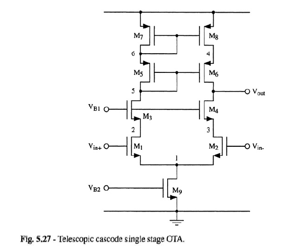
Let's consider, for example, this circuit:

enter image description here

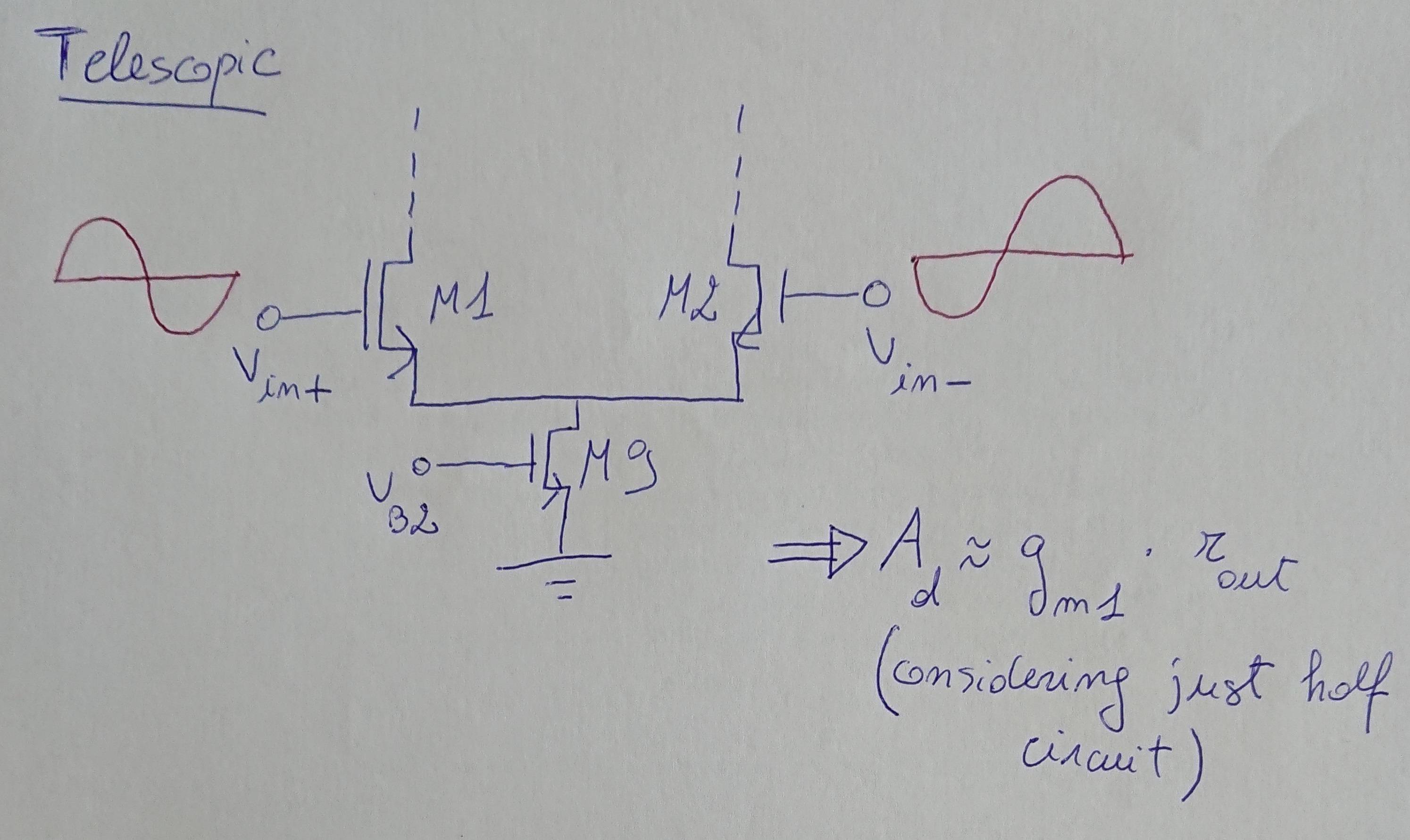
During lessons, our professor always assumed perfect differential input (two signals with the same dc value and with equal and opposite amplitudes). As a consequence node 1 will be an ac ground due to symmetry and the small signal differential gain can be easily found:

enter image description here

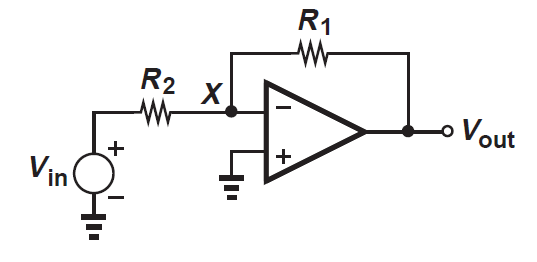
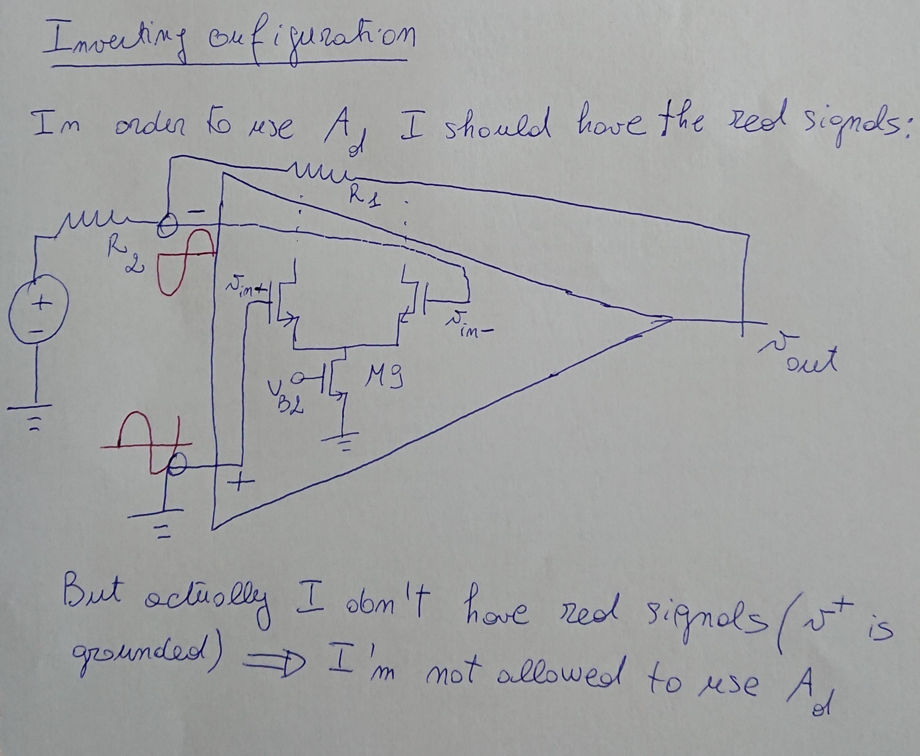
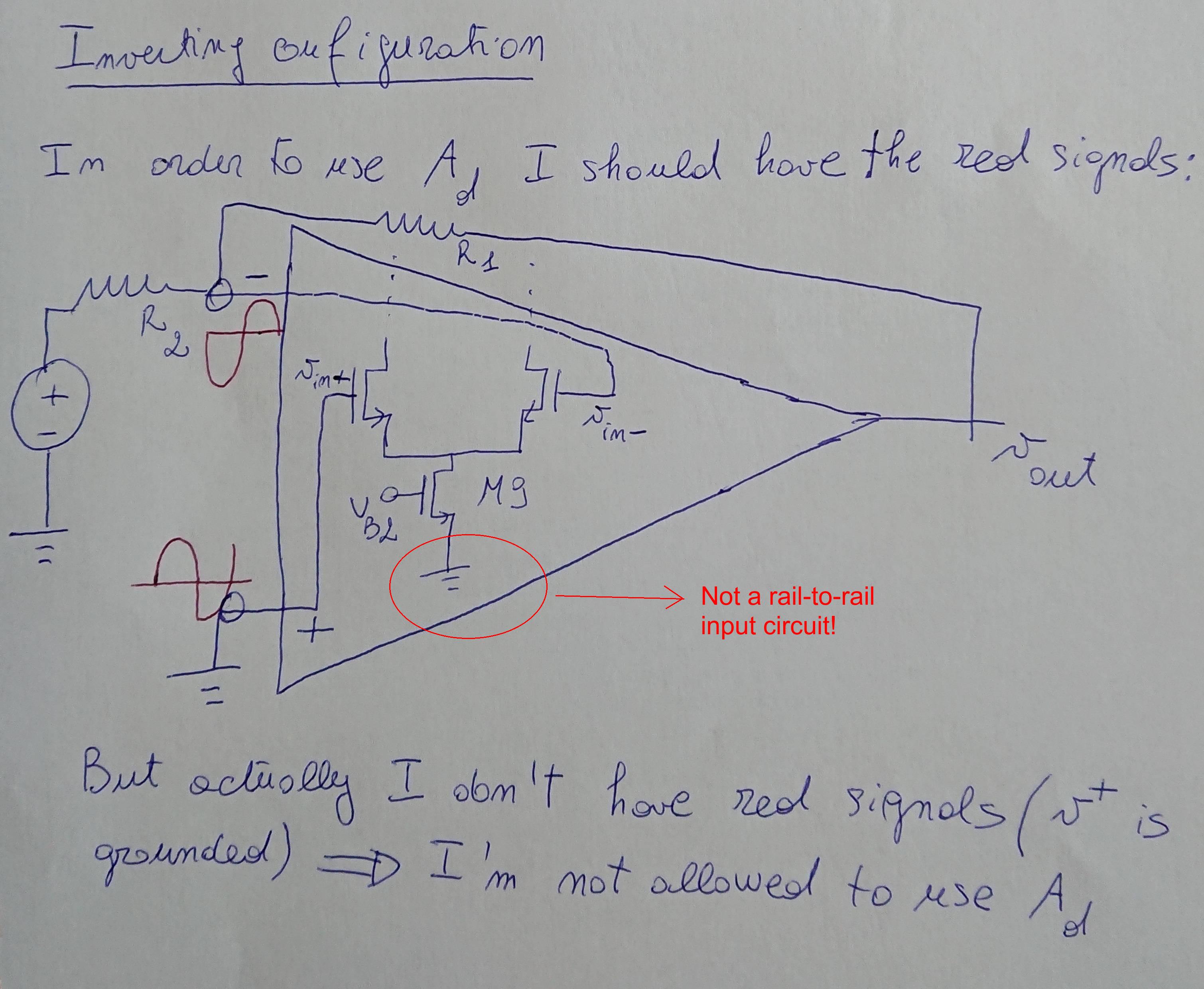
Now the question: when I close this circuit (or in general every circuit with a differential pair stage, which is the input block of an op-amp) with negative feedback, I will not have a perfect differential input, thus I am not allowed to use the previous differential gain (which was actually found under the assumption of differential input). Let's consider for example this basic circuit:

enter image description here

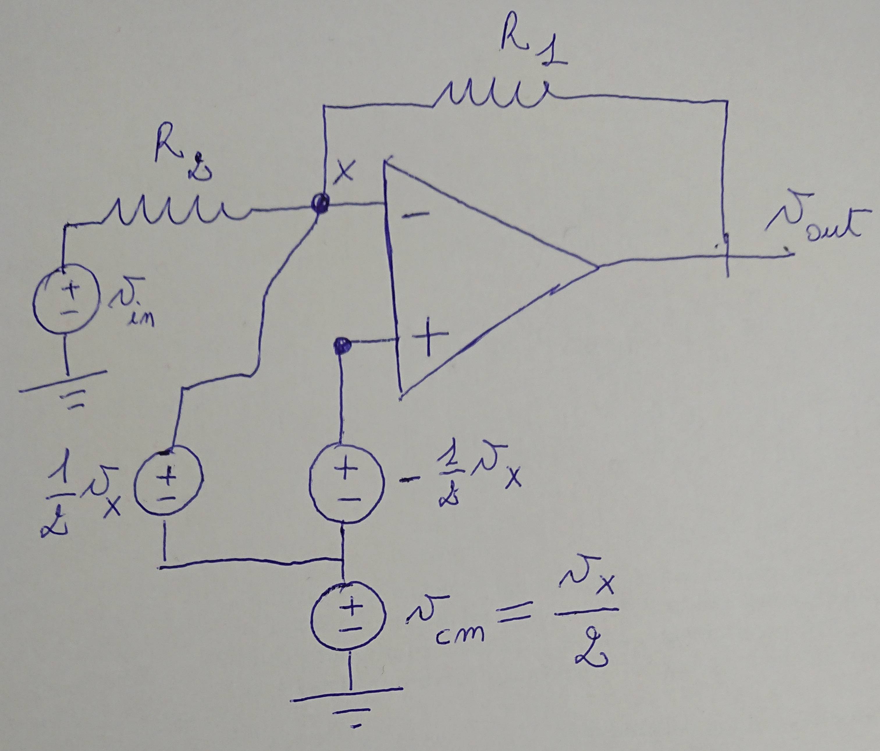
You can see that the non-inverting terminal is fixed to the analog ground, thus it can not change in a differential way with respect to the inverting terminal. In a similar question I wrote, I've been answered that actually you can always write a couple of signals as the sum of a common mode signal and a differential signal, and since a well-designed op-amp has a common mode gain wihich is much smaller than the differential gain, we can neglect the common mode gain (and thus use only the previous expression for the differential gain). Now I would like to have some hints on how to proceed with the analysis in this case. For example, considering the previous inverting configuration, I tried to decompose the input of the op-amp:

enter image description here

where vx is the voltage at the inverting terminal. Is it correct? How to proceed with the analysis?

Thank you

Edit for the comment:

For the telescopic configuration, the differential gain was found under the hypothesis of differential input signals:

enter image description here

When we close the feedback around it we get:

enter image description here

\$\endgroup\$
1
  • \$\begingroup\$ But did you manage to computed the of a diff amp for this case? Is there any practical difference in the finally value? Also if you ground the gate of a first mosfet and apply the input signal to M2 gate. We can still write Vin = Vid = Vgs2 + Vsg1 and because M1 and M2 are identical Vgs1 = Vid/2 and Vsg2 = Vid/2 (Vsg2 = - Vgs1) So, you can be worried or not? \$\endgroup\$
    – G36
    Commented Jul 26, 2019 at 14:42

2 Answers 2

2
\$\begingroup\$

Brief Background
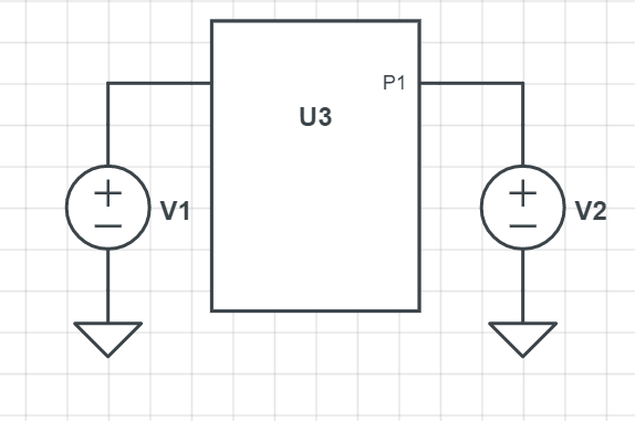
Suppose you have a linear network which has two input ports with input voltages \$V_1\$ and \$V_2\$ as shown in figure below:

enter image description here

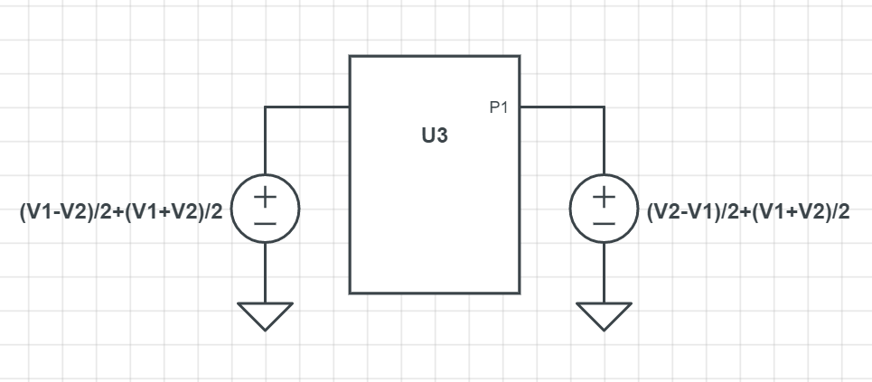
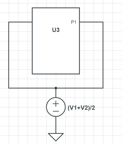
Then, since \$V_1 = \frac{V_1-V_2}{2}+\frac{V_1+V_2}{2}\$ and \$V_2=\frac{V_2-V_1}{2}+\frac{V_1+V_2}{2}\$. Thus we have:

enter image description here

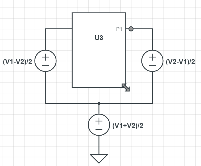
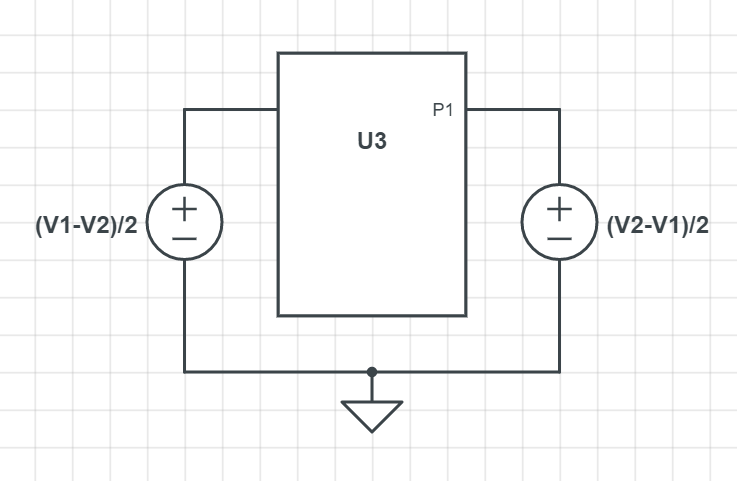
Then you can transform the circuit as shown below:

enter image description here

Here the common mode voltage is: \$V_{cm} = \frac{V_1+V_2}{2}\$ and the differential voltage is: \$\frac{V_{diff}}{2} = \frac{V_1-V_2}{2}\$. Since the circuit is linear, superposition is valid. So we can say that the total response will be sum of these two.

enter image description here

enter image description here

The first one is the the common-mode circuit and the second one is the differential circuit. Here you can use all the tricks for the differential half and the common-mode half which you may know.
Your Example
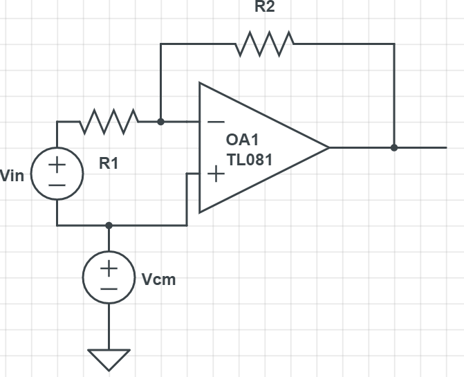
The complete circuit for the example you provided will be:

enter image description here

Here the two inputs are: \$V_1=V_{cm}+V_{in}\$ and \$V_2 = V_{cm}\$.
If you use superposition here with \$V_{cm}=0\$, you get the circuit which you have shown in your question. This is the differential part of the circuit.
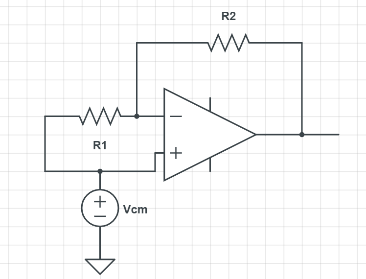
If you instead make \$V_{in}=0\$, you get the common-mode circuit: enter image description here

I leave it to you now to analyze it.

\$\endgroup\$
7
  • \$\begingroup\$ I read and understood the "brief background" section, but I don't understand "your example" section. What do you mean with "differential part" and who are V1 and V2 in the inverting configuration? Again thank you \$\endgroup\$
    – Stefanino
    Commented Jul 26, 2019 at 10:21
  • 1
    \$\begingroup\$ @Stefanino Please see the edits. Hope this clarifies things. If not, let me know. \$\endgroup\$
    – sarthak
    Commented Jul 26, 2019 at 11:08
  • \$\begingroup\$ I thank you for the edit, now it is much more clear. However the doubt still remains in me: when you split the two input signals (vin and ground) into common mode signal and differential signal, you still don't have at the input terminals of the op-amp a perfect differential (or perfect common) signal, because you have a voltage drop on R1. Instead in the telescopic circuit (for example) you have a differential signal ditectly applied to input terminals. Thus, in your differential part circuit, who says I can use Ad (i.e. the differential gain)? I hope I was clear. Thank you for your patience! \$\endgroup\$
    – Stefanino
    Commented Jul 26, 2019 at 12:09
  • \$\begingroup\$ I also added two pictures to my question in order to be more clear \$\endgroup\$
    – Stefanino
    Commented Jul 26, 2019 at 12:43
  • \$\begingroup\$ @Stefanino The gain is the same for a differential input and single ended output amplifier. You would have a schematic like this: google.com/…: \$\endgroup\$
    – sarthak
    Commented Jul 26, 2019 at 13:13
2
\$\begingroup\$

I considered very positive your patience to restate the question you posted before, and, like others, I thought that the problem was your concept of "perfect differential input". May I suggest that you evaluate that, in fact, the differential input stage that you consider in your analysis is simply not rail-to-rail capable? Please kindly take a look at the modified picture:

enter image description here

If you want to connect one of these inputs to \$0 V\$ you should consider your input stage powered by split supplies (e.g. \$\pm 15 V\$).

\$\endgroup\$
5
  • \$\begingroup\$ Yes, you're right, that node must be connected to VSS and not ground. However, even if I adjust the schematic as you correctly said, my doubt still exists: in order to use Ad, we should have those red differential signals (because Ad was found under that hypothesis); how to prove (if I am right) that they are differential? Thank you \$\endgroup\$
    – Stefanino
    Commented Jul 26, 2019 at 13:26
  • 1
    \$\begingroup\$ I see your point. Thanks for clarifying. The lack of symmetry would break the "ac ground" assumption that facilitates the differential gain analysis. \$\endgroup\$
    – devnull
    Commented Jul 26, 2019 at 13:46
  • \$\begingroup\$ +2 I was going to comment on this but see that you point it out neatly. From the first reading and the OPs first diagram I was nervous about below rail input operation and erroneous assumptions leading from there as a start. \$\endgroup\$
    – KalleMP
    Commented Jul 26, 2019 at 21:14
  • \$\begingroup\$ I made a mistake because I copied the schematic of my book, but this is not the problem: obviously the source of M9 must be connected to a negative voltage. The doubt I have still remains: how can be proved (if I'm right) that the red signals are differential? \$\endgroup\$
    – Stefanino
    Commented Jul 27, 2019 at 8:29
  • \$\begingroup\$ In the last picture (with corrections made...), you can not say that the red signals are "differential" because one point is grounded. You can speack only of an "error input" which can permit the OPamp to be functional. You can split eventually this "error" in differential and common mode signals while redesigning theoritical schematic. But no need to do so. Input - is a virtual ground. So Ad can be used. \$\endgroup\$
    – user288518
    Commented Jun 15, 2021 at 8:30

Your Answer

By clicking “Post Your Answer”, you agree to our terms of service and acknowledge you have read our privacy policy.

Not the answer you're looking for? Browse other questions tagged or ask your own question.