0
\$\begingroup\$

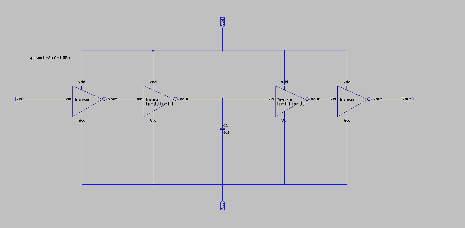
I'm trying to design an integrated circuit that can implement a delay of approximately 100 ns, working with a 180nm process. With this process, an inverter has a delay of picoseconds, so it would require too many of them in a chain to achieve such a delay. I decided to use the following circuit

enter image description here

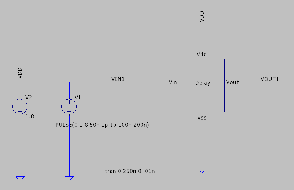
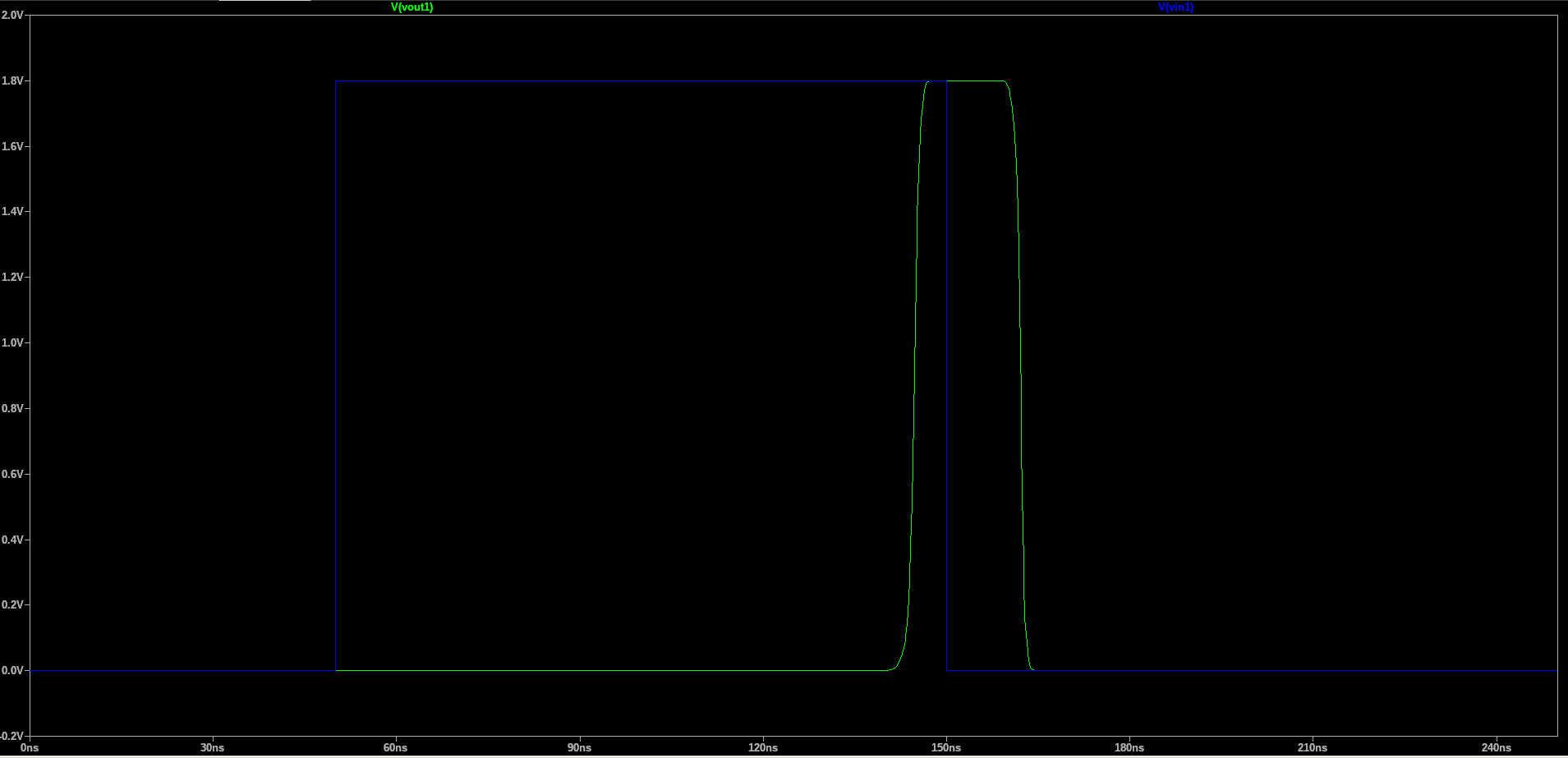
It is acheiving the delay I was looking for. However, the delay is just for the low-to-high transition, in the high-to-low the delay is much lower, and I can't understand way. Here are figures of the circuit used for simulation and the results

enter image description here enter image description here

Any explanation for the behaviour? I was expecting it to have the same delays. The inverters are ratioed Wp/Wn = 2 to achieve symmetrical propagation delays.

\$\endgroup\$
7
  • \$\begingroup\$ "The inverters are ratioed Wp/Wn = 2 to achieve symmetrical propagation delays." - So are they symmetrical (without the capacitor)? Have you measured the model's source and sink currents? \$\endgroup\$ Commented Feb 4, 2020 at 6:29
  • \$\begingroup\$ Normally slew rate is limited by Ron @ Vdd. This suggests your Pch is mismatched high . \$\endgroup\$
    – D.A.S.
    Commented Feb 4, 2020 at 8:57
  • \$\begingroup\$ @BruceAbbott, I have simulated the propagation times for an inverter with no charge and they are indeed symmetrical, I can provide the results of the simulations later. \$\endgroup\$
    – MPA95
    Commented Feb 4, 2020 at 17:11
  • \$\begingroup\$ @TonyStewartSunnyskyguyEE75 You mean a mismatch in the widths? Is that possible if the propagation delays are the same for the inverter? \$\endgroup\$
    – MPA95
    Commented Feb 4, 2020 at 17:12
  • \$\begingroup\$ I suspect that the fact that only the second inverter has a considerable capacitance at its output is causing this, is this theory plausible? \$\endgroup\$
    – MPA95
    Commented Feb 4, 2020 at 17:13

1 Answer 1

3
\$\begingroup\$

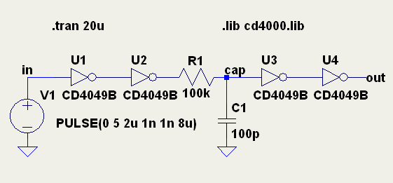
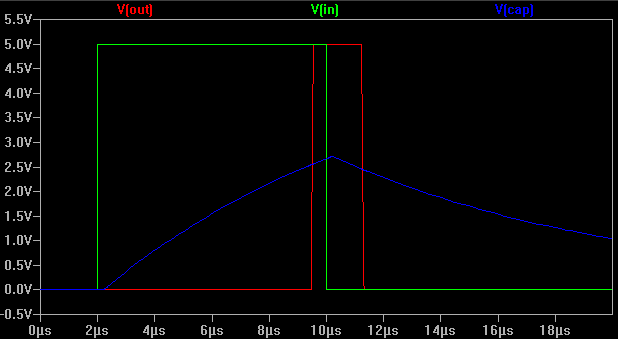
I think the problem is simply that the pulse is too short to charge the capacitor fully. I created a simulation using CD4000 series inverters at a time scale long enough that propagation delays are insignificant, and with an external resistor to ensure symmetrical output resistance. It showed the same effect as your circuit.

enter image description here

enter image description here

With this short pulse length (relative to the delay time) the capacitor barely has enough time to charge above the gate input threshold before the pulse ends, then it only has to discharge a little bit to get below the threshold again. The result is much shorter delay after the falling edge of the pulse than the leading edge.

If the pulse was longer or the on/off ratio was closer to 50% the delays would be more symmetrical, but if you need to delay a short intermittent pulse while maintaining its width this technique is not suitable.

\$\endgroup\$

Your Answer

By clicking “Post Your Answer”, you agree to our terms of service and acknowledge you have read our privacy policy.

Not the answer you're looking for? Browse other questions tagged or ask your own question.