8
\$\begingroup\$

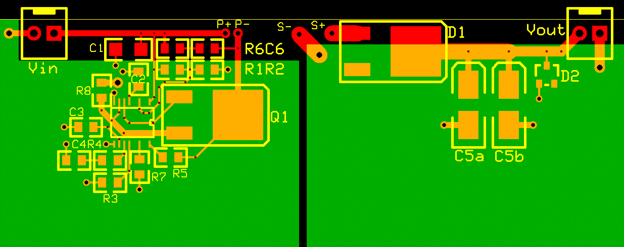
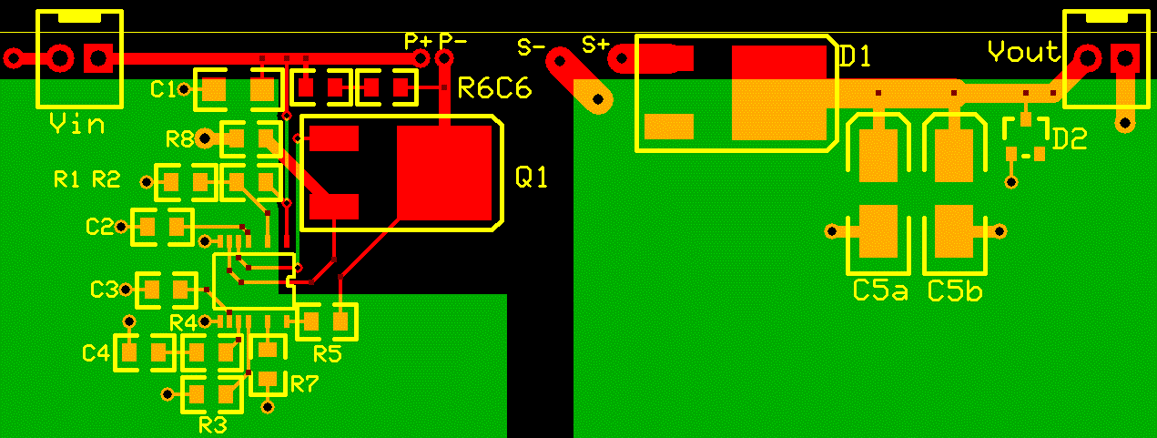
This is kind of 3rd in a series, following the posts Advice on ground plane in my first PCB and then Separating ground planes in PCBs. In terms of material, though, it can be considered a post on its own. So to summarize the PCB below (prepared using ExpressPCB) is for a flyback converter implementation using the LT3748 boundary mode flyback controller IC. The circuit is taken from the LT3748 datasheet itself (see very last page). This is for a class project.

I have attempted an improved PCB based on advice in previous posts. I have two versions, shown below.
enter image description here

enter image description here

My questions are:

  1. The switching loop goes around the controller (since the tracks go under the IC - but in the same layer of the IC). Is this very bad for noise? BTW, would you consider the switching loop to be Vin-xformer-Q1-R8, or C1-xformer-Q1-R8?

  2. For top version, all tracks are on top layer only, but many of them go under the IC (on the same top layer). Is that bad practice? I cannot guarantee the IC won't heat up since the datasheet quotes performance at temperatures up to 150 C.

  3. I have only one ground on the primary side. I'm not sure how in my situation to keep a separate ground for the small-signal and high-current loops. I can do but this will put a few breaks in my ground plane...

Finally, as a note, another difficult constraint I was trying to meet is that the controller datasheet says the sense resistor (R8) ground should be close to controller IC, but at the same time to keep the switching loop tight R8 needs to be close to the capacitor.

Keeping all of this in mind, which design would you think would perform better - or is it neither :) Note that teh second design has a few tracks on the bottom layer (green).

\$\endgroup\$
4
  • 11
    \$\begingroup\$ Guys, he is learning.. Please do not be harsh on him with things like "Why don't you use reference design?". I really understand him and I was like this one day, of course with DC/DC converters, I do not know anything about switching AC/DC conversion.. \$\endgroup\$ Commented Nov 27, 2012 at 15:58
  • 3
    \$\begingroup\$ @LeonHeller Teach a man to fish, etc, etc... \$\endgroup\$
    – dext0rb
    Commented Nov 27, 2012 at 16:21
  • 3
    \$\begingroup\$ @abdullahkahraman Agree with you. There's demonstrated skill improvement going on here. \$\endgroup\$ Commented Nov 27, 2012 at 16:29
  • \$\begingroup\$ Thanks to all for useful comments. I cannot follow exactly datasheet PCB layout because, as mentioned in previous post, I am using an external transformer. Nevertheless, I followed many of suggested guidelines like placing feedback resistors (R5 and R7) v close to IC, placing ground of R8 (sense resistor) near IC, and keeping switching loops small in area (C1-priamry-Q1-R8 and C2-Q1-R8). Also followed other suggestions to my previous posts like keeping R8 v close to C1. Will study more other LT3748 demo board layouts, but in mean time would appreciate answers to my 3 questions above. \$\endgroup\$ Commented Nov 28, 2012 at 19:19

1 Answer 1

1
\$\begingroup\$
  1. You want the ESR of C1 to be much lower than the V1 so the loop is small. You also want it lower than Q1 rON to be reduce input ripple.

  2. Top one is hard to analyze as the ground plane helps Q1 but then gap becomes a slotted ground radiator antenna.

I think neither is better as the external transformer is going to be excessively noisy and ferrite CM chokes will be mandatory to reduce radiation of Vout cables acting as noisy antenna.

I suggest you perform a bench test using a generator to drive Q1 C1 with Rs & transformer & output fully loaded (D,C,R). YOu don't need a PCB to test this EMI problem and see if you can measure the sense current and output accurately without noise and verify EMI egress with a shorted loop scope probe for near field noise. Designing a PCB without this awareness will be pointless.

\$\endgroup\$
2
  • \$\begingroup\$ Thakn you, Richman, for your useful comments. Regarding #2, should I reshape my ground planes? Also where would you suggest placing the ferrite CM chokes - at input and outpout at terminals, or other locations too? \$\endgroup\$ Commented Nov 28, 2012 at 19:24
  • \$\begingroup\$ In order to prevent EMI issues with any high impedance circuits nearby, I would put on output to suppress radiation. Input cable will also radiate so depends on system design overall. Use twisted pairs for both. \$\endgroup\$
    – D.A.S.
    Commented Nov 28, 2012 at 19:36

Your Answer

By clicking “Post Your Answer”, you agree to our terms of service and acknowledge you have read our privacy policy.

Not the answer you're looking for? Browse other questions tagged or ask your own question.