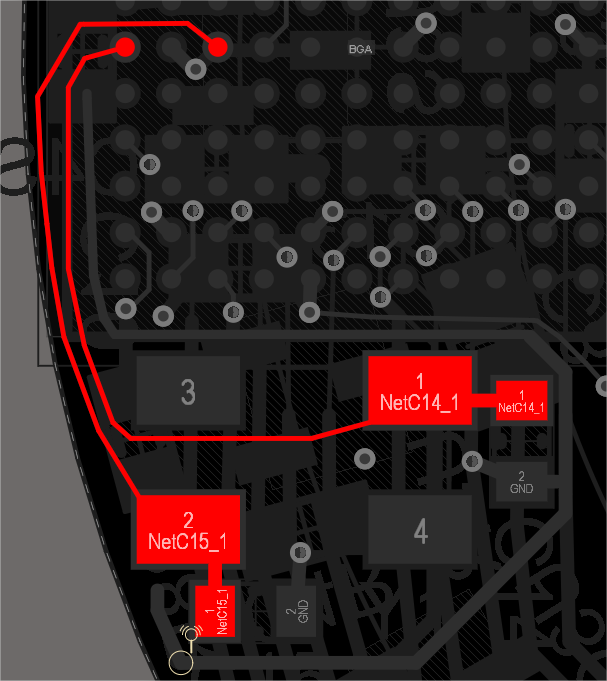
I'm designing a PCB with 8MHz crystal for DSPIC33EP512MU810-E/BG (https://www.digikey.com/product-detail/en/microchip-technology/DSPIC33EP512MU810-E-BG/DSPIC33EP512MU810-E-BG-ND/2765491)
On the datasheet, recommendations say that my traces should not exceed 12mm but this is the best I can do since my PCB board is defined and can't be changed.The crystal is side by side with the uC.
I have a ground plane below the crystal and the GND polygon pour around the crystal is 7mil.
Do you guys see any issue with this Crystal layout ?
Thanks,


