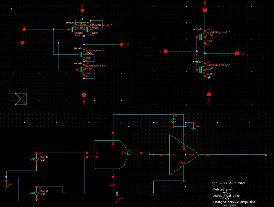
 I am designing a simple circuit where I want to use the output of one NAND as the input to a NOT gate. I have implemented both the gates using CMOS (NOT with 2 MOSFETs and NAND with 4 MOSFETs). Both of my gates are working fine separately. But when I combine them and give a square wave as an input the output is very weird. I am new to this and am just trying to figure out things. Can anyone please tell me what am I doing wrong?
-
4\$\begingroup\$ Post your schematic for starters. Also define a "very weird" output. \$\endgroup\$– Eugene Sh.Commented Apr 16, 2021 at 18:20
-
\$\begingroup\$ Are your n- and p-FETs in the right places? That is, p-FETs with source tied to VDD, n-FETs with source tied to VSS or towards it? See this Q: electronics.stackexchange.com/questions/560142/… \$\endgroup\$– hacktasticalCommented Apr 16, 2021 at 18:26
-
\$\begingroup\$ Are you simulating or did you build an actual circuit? If you built an actual circuit, can you post a picture of it? The picture will answer 1000 questions that we would otherwise need to ask. The schematic would also be very helpful. \$\endgroup\$– user57037Commented Apr 16, 2021 at 18:32
-
2\$\begingroup\$ Show us a picture of "very weird". \$\endgroup\$– Elliot AldersonCommented Apr 16, 2021 at 18:52
-
1\$\begingroup\$ Tip: a point on good schematics. Your lower schematic has many unnecessary kinks and crossovers which make it much more difficult to read than it should be. (1) Remove all ground nets and just use the gnd symbol at each grounded node. That will eliminate 12 lines from your drawing. (2) Line up components and nets to minimise kinks and crossovers. If you are interested in improving, Rules and guidelines for drawing good schematics is well worth a read. (3) Black on white is better. \$\endgroup\$– TransistorCommented Apr 16, 2021 at 19:00
2 Answers
The logic gates must have low output impedance and high input impedance, otherwise the logic circuit formed by connecting these gates will not work properly, also each of them, as a standalone circuit, may function as desired because the oscilloscopes or the multimeters have high input impedances.
In other words if the the second gate draws a lot of current from the output of the first, both circuits will malfunction.
You need to research pull up and pull down resistors with logic gates. Btw, your NAND gate appears to be missing a pull down resistor on its output.
