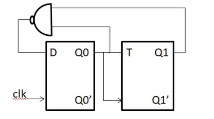
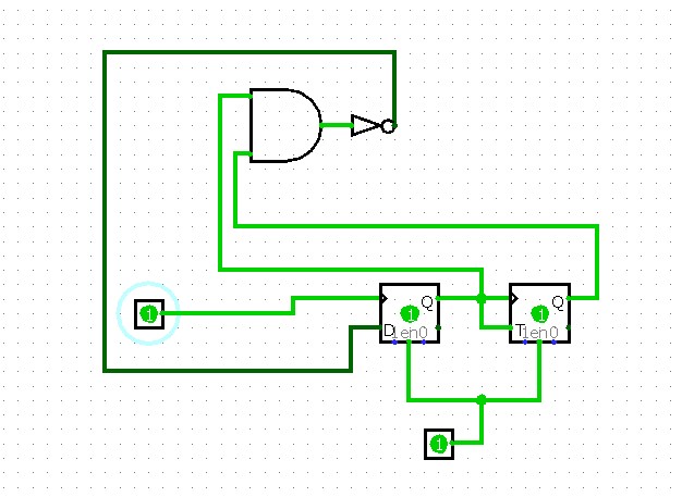
It is given that Q0[MSB] and Q1[LSB] are both 0 initially and the circuit is edge triggered. The answer says this circuit will generate 2, but I am arriving at 3 and I can't see where I am going wrong.
My thought process is, initially Q0 and Q1 are 0, so the NAND gate will output one, therefore input to D will be 1. When the clock pulse is applied, 1 will pass through the D-Flip Flop and we will have Q0 = 1, now since Q0 is the input to the CLK of the T-Flip Flop and it has gone from 0 to 1, the T-Flip Flop will be activated, Q0 = 1 is also input to T, so it will toggle Q1 = 0 to Q1 = 1, and we will finally have Q0 = 1 and Q1 = 1, which is 3.
My instructor's explanation for arriving at 2:
"we always consider the initial states as the input to the flip-flops. The Q0n and Q1n are the next state values that we get as the output from the flip flop. Please don't get confused with this.
The input to the T-FF is Q0 and not Q0n. For Q1 = Q0 = 0 Input to the D-FF is (Q0 . Q1)' = (0. 0)' = 1 This makes the Q0n = 1 But this Q0n is not the input to the T-FF. Input to the T flip flop is Q0, and it will be active only when Q0 -> Q0n = 0 -> 1. Since for the case Q0 = Q1 = 0, Q0->Q0n is 0 -> 1, therefore, T-FF will be active. Input to the T-FF is Q0 = 0, therefore, it will latch the Q1. Hence, Q1n = 0."


Tand clock. AFAIK, the input should appear slightly earlier than the clock edge. See Timing section in this article. I am not sure though. Are these concepts taught by your instructor? \$\endgroup\$T=0. But, I would either 1) wait for someone to answer this question where it is accounted for, or 2) try to do a simulation that takes this into account or 3) look up a text book where a problem which takes this into account is worked out clearly. Especially since a answer containing a simulation result is posted which says otherwise. \$\endgroup\$